| . |  |
. |
| . | |
. |
|
by Staff Writers Munich, Germany (SPX) Feb 20, 2019
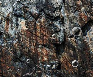
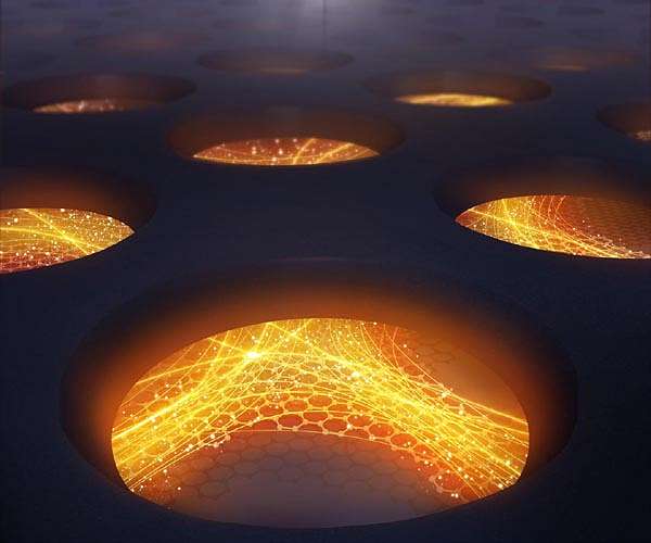
Graphene Flagship researchers solved one of the challenges of making graphene nano-electronics effective: to carve out graphene to nanoscale dimensions without ruining its electrical properties. This allowed them to achieve electrical currents orders of magnitude higher than previously achieved for similar structures. The work shows that the quantum transport properties needed for future electronics can survive scaling down to nanometric dimensions. Since its inception, scientists have tried to exploit graphene to produce nano-sized electronics. However, since graphene is only an atom thick, all atoms are exposed to the outside world, and even small amounts of defects and impurities impede its properties. Now, Graphene Flagship researchers at DTU, Denmark solved this problem by protecting graphene with insulating layers of hexagonal boron nitride, another two-dimensional material with insulating properties. Peter Boggild, researcher at Graphene Flagship partner DTU and coauthor of the paper, explains that although 'graphene is a fantastic material that could play a crucial role in making new nano-sized electronics, it is still extremely difficult to control its electrical properties.' Since 2010, scientists at DTU have tried to tailor the electrical properties of graphene, by making a very fine pattern of holes, so that channels through which an electric power can flow freely are formed. 'Creating nanostructured graphene turned out to be amazingly difficult, since even small errors wash out all the properties we designed it to have,' comments Boggild. Now, researchers from Graphene Flagship partner DTU made a leap forward. Bjarke Jessen and Lene Gammelgaard encapsulated graphene with another 2D material, hexagonal boron nitride, which is very similar to graphene, but electrically insulating. Then, using nanolithography, they carefully drilled nanoscopic holes in graphene through the protective layer of boron nitride. The holes have a diameter of approximately 20 nanometers, and are separated from each other with just 12 nanometers. This great precision makes possible to send an electrical current through the graphene that is 100-1000 times higher than typical numbers for lithographically carved nanographene. 'When you make patterns in a material like graphene, you do so in order to change its properties. However, what we have seen throughout the years is that when we shape graphene on this fine scale, it does not behave like graphene anymore - there is too much disorder,' explains Boggild. 'Many scientists have abandoned nanolithography in graphene on this scale, but now we have figured out how it can be done - you could say that the curse is lifted,' he adds. 'We have shown that we can control graphene's band structure and that deterministic design of nanoelectronics is realistic. Looking solely at electronics, this means that we can make insulators, transistors, conductors and perhaps even superconductors, as our nanolithography can preserve the subtle inter-layer physics that was recently shown to lead to superconductivity in double-layer graphene. However, it goes way beyond that. When we control the band structure, we have access to all of graphene's properties. In other words, we could sit in front of the computer and dream up other applications - and then go to the laboratory and make them happen,' says Boggild. 'There are plenty of practical challenges, but the fact that we can tailor electronic properties of graphene is a big step towards creating new electronics with extremely small dimensions,' he concludes. Daniel Neumaier, Graphene Flagship Division Leader for Electronics and Photonics Integration says: 'Controlling the electronic properties of graphene by nano-pattering offers an additional degree of freedom for the design of electronic and photonic devices, which was so far not accessible. The researchers from Graphene Flagship partner DTU and their co-workers now discovered a unique way for nano-patterning of graphene without seeing the limitations of patterning introduced defects. This was the key enabling step for using the nano-patterning induced electronic properties of graphene in real device and we are expecting significant advances especially for nano-electronics and photonics based on these results.' Andrea C. Ferrari, Science and Technology Officer of the Graphene Flagship and Chair of its Management Panel added how 'patterning of graphene to create nano-electronic devices was one of the first approaches attempted to exploit this unique material into devices. However, after an initial flurry of publications, the amount of damage produced was so much that this line of research was almost entirely abandoned. The work presented here shows how the long term nature of the Flagship allows scientists to pursue and solve even apparently intractable problems. This will rejuvenate the interest in graphene nanoelectronics, and could lead to a variety of useful devices, previously hampered by defects.'
Carbon gas storage cavern is the best way to obtain clean energy from a fossil fuel Sao Paulo, Brazil (SPX) Feb 14, 2019 A set of technologies that is expected to have its first results four years from now is designed to resolve one of the world's greatest oil and gas exploration challenges today: carbon dioxide (CO2) and methane (CH4) emission in the atmosphere. The innovation, the result of a patent deposited in 2018, consists of injecting the CO2 and CH4 that comes from wells during oil extraction into salt caverns as a way to reduce the amount of carbon gas in the emissions. The first "pilot cavern" may be ... read more
|
|||||||||||||
| The content herein, unless otherwise known to be public domain, are Copyright 1995-2026 - SpaceDaily. All websites are published in Australia and are solely subject to Australian law and governed by Fair Use principals for news reporting and research purposes. By using our websites you consent to cookie based advertising. If you do not agree with this then you must stop using the websites from May 25, 2018. Privacy Statement. Additional information can be found here at About Us. |
 del.icio.us
 Digg
Digg Reddit
 Google