| . |  |
. |
| . | |
. |
|
by Staff Writers University Park PA (SPX) Apr 30, 2018
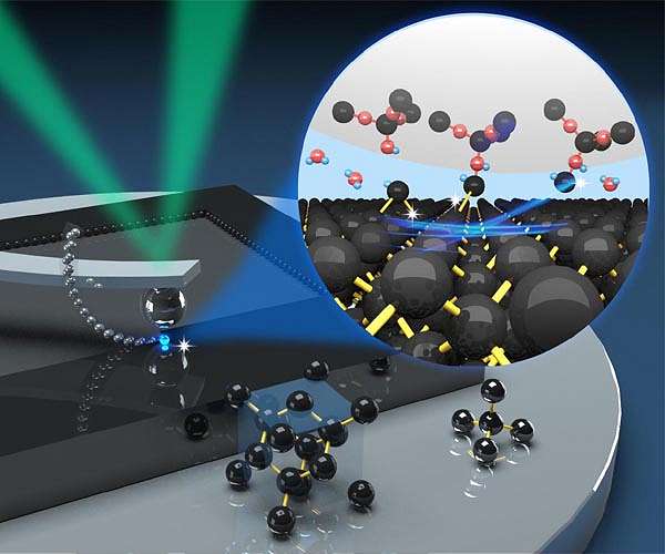
A precise, chemical-free method for etching nanoscale features on silicon wafers has been developed by a team from Penn State and Southwest Jiaotong University and Tsinghua University in China. In standard lithography, a photosensitive film is deposited on a silicon wafer and a pattern called a mask is used to expose certain portions of the film. Then, chemicals - such as a potassium hydroxide solution - etch patterns into the silicon. Further steps are required to smooth out the roughened surface. The Penn State and Southwest Jiaotong University researchers developed an entirely different, chemical- and mask-free, one-step process. They lightly rubbed a rounded silica tip of an instrument called a scanning probe microscope across a silicon substrate - the material base typically used to make electronic devices. When exposed to the water vapor in air, the top layer of silicon forms bonds with the tip of the scanning probe, and a single layer of atoms slides off as the probe moves across the silicon. Because the atoms below do not take part in the chemical reaction, they are completely undamaged. "It's really quite a unique idea," said Seong Kim, professor of chemical engineering, Penn State. "It's a so-called tribochemical reaction. Unlike chemical reactions caused by heat, light or electric fields, which are all widely studied, mechanically-stimulated chemical reactions are less understood." The removal mechanism is initiated when the silicon is exposed to air and the top atomic layer of silicon atoms reacts with water molecules to make silicon-oxygen-hydrogen bonds. Then the silicon oxide surface of the tip forms a silicon-oxide-silicon bond with the substrate surface under the shear force of the moving tip. This facilitates the removal of the silicon atom from the topmost surface of the substrate. People in nanofabrication who are trying to reduce the size of device features down to atomic-scale dimensions could find this technique useful, Kim believes. "Atomic layer etching can provide the depth resolution that people would like to get without the use of sacrificial layers and harsh chemicals," he said. This kind of patterning method is too slow for microfabrication now, Kim acknowledged. However, researchers could use it to create a platform for testing electronic and microelectromechanical devices with features at the Angstrom or single-atom scale, far smaller than current devices. At least one company, IBM, has experimented with multiple probe arrays that could lead to large-scale patterning of devices. "Our process could be combined with their process to scale up," Kim said. "This is the initial science part. Once we see the science, a lot of possibilities can be explored. For instance, we think this technique will work with other materials beyond silicon." The researchers describe their technique in Nature Communications in an article titled "Nanomanufacturing of Silicon Surface With a Single Atomic Layer Precision Via Mechanochemical Reactions."
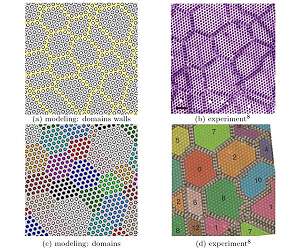
Similar charges are attracted to each other Moscow, Russia (SPX) Apr 22, 2018 NUST MISIS scientists have finally found out why a material that could potentially become the basis for ultra-fast memory in new computers is formed. Professor Petr Karpov and Serguei Brazovskii, both researchers at NUST MISIS, have managed to develop a theory which explains the mechanism of the latent state formation in layered tantalum disulfide, one of the most promising materials for modern microelectronics. The latent state of matter (which will be discussed further) was discovered by Serguei ... read more
|
|||||||||||||
| The content herein, unless otherwise known to be public domain, are Copyright 1995-2026 - SpaceDaily. All websites are published in Australia and are solely subject to Australian law and governed by Fair Use principals for news reporting and research purposes. By using our websites you consent to cookie based advertising. If you do not agree with this then you must stop using the websites from May 25, 2018. Privacy Statement. Additional information can be found here at About Us. |
 del.icio.us
 Digg
Digg Reddit
 Google