| . |  |
. |
| . | |
. |
|
by Staff Writers Berlin, Germany (SPX) Jul 25, 2017
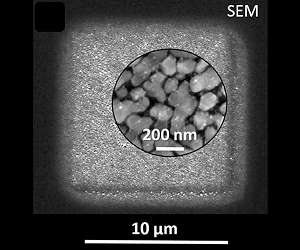
When it comes to extremely fine, precise features, a scanning electron microscope (SEM) is unrivaled. A focused electron beam can directly deposit complex features onto a substrate in a single step (Electron-Beam-Induced Deposition, EBID). While this is an established technique for gold, platinum, copper and further metals, direct electron beam writing of silver remained elusive. Yet, the noble metal silver promises especially interesting potential applications in nano-optics in information technology. For the first time a team from the HZB and the Swiss Federal Laboratories for Materials Science and Technology (EMPA) has successfully realized the local deposition of silver nanocrystals by EBID. The results have now been published in the journal of the American Chemical Society's ACS Applied Materials Interfaces. The chemistry of typical silver compounds is extremely challenging. They are difficult to evaporate and are highly reactive. During the heating in the injection unit, they tend to chemically react with the reservoir walls. Along their path from the reservoir to the tip of the needle, these compounds freeze again at the slightest drop in temperature and obstruct the tube. "It took us a lot of time and effort to design a new injection unit and find a suitable silver compound", explains HZB physicist Dr. Katja Hoflich, who carried out the experiments as part of a Helmholtz Postdoctoral Fellowship at EMPA. "Finally, we managed it. The compound silver dimethylbutyrate remains stable and dissociates only in the focus of the electron beam." Hoflich and her colleagues used the EBID method to create sharply defined areas of tiny silver nanocrystals for the first time.
Writing with the electron beam
Silver is a light concentrator This effect can be utilised in Raman spectroscopy to detect the fingerprint of specific molecules that bind to the silver surface - down to the level of a single molecule. Hence, silver nanostructures are good candidates as sensors for explosives or other dangerous compounds.
A vision for the future: components for optical computing The results have now been published in ACS Applied Materials and Interfaces (2017): "Direct Electron Beam Writing of Silver-Based Nanostructures". Katja Hoflich, Jakub Jurczyk,Yucheng Zhang, Marcos V. Puydinger dos Santos,,Maximilian Gotz, Carlos Guerra-Nunez, James P. Best,Czeslaw Kapusta, and Ivo Utke.
 Making telescopes that curve and twist
Los Angeles CA (SPX) Jul 24, 2017 A new tool for computational design allows users to turn any 3D shape into a collapsible telescoping structure. New mathematical methods developed by researchers at Carnegie Mellon University capture the complex and diverse properties of such structures, which are valuable for a variety of applications in 3D fabrication and robotics--particularly where mechanisms must be compact in size and easi ... read more Related Links Helmholtz-Zentrum Berlin fur Materialien und Energie Space Technology News - Applications and Research
|
|||||||||||||
| The content herein, unless otherwise known to be public domain, are Copyright 1995-2026 - SpaceDaily. All websites are published in Australia and are solely subject to Australian law and governed by Fair Use principals for news reporting and research purposes. By using our websites you consent to cookie based advertising. If you do not agree with this then you must stop using the websites from May 25, 2018. Privacy Statement. Additional information can be found here at About Us. |
 del.icio.us
 Digg
Digg Reddit
 Google