| . |  |
. |
| . | |
. |
|
by Staff Writers Dallas TX (SPX) Mar 21, 2017
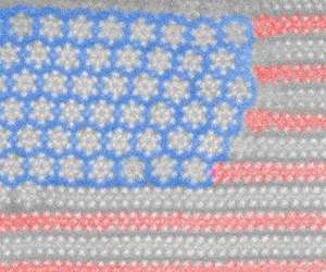
For several years, a team of researchers at The University of Texas at Dallas has investigated various materials in search of those whose electrical properties might make them suitable for small, energy-efficient transistors to power next-generation electronic devices. They recently found one such material, but it was nothing anyone expected. In an article published online March 10 in the journal Advanced Materials, Dr. Moon Kim and his colleagues describe a material that, when heated to about 450 degrees Celsius, transforms from an atomically thin, two-dimensional sheet into an array of one-dimensional nanowires, each just a few atoms wide. An image caught in mid-transformation looks like a tiny United States flag, and with false colors added, is arguably the world's smallest image of Old Glory, Kim said. "The phase transition we observed, this new structure, was not predicted by theory," said Kim, the Louis Beecherl Jr. Distinguished Professor of materials science and engineering at UT Dallas. Because the nanowires are semiconductors, they might be used as switching devices, just as silicon is used in today's transistors to turn electric current on and off in electronic devices. "These nanowires are about 10 times smaller than the smallest silicon wires, and, if used in future technology, would result in powerful energy-efficient devices," Kim said. The lead authors of the study are Hui Zhu and Qingxiao Wang, graduate students in materials science and engineering in the Erik Jonsson School of Engineering and Computer Science.
Just a Phase? For many materials, however, a phase transition means something a little different. As external temperature and pressure change, these materials' atoms rearrange and redistribute to make a material with a different structure and composition. These changes can affect the new material's properties, such as how electrons move through it. For scientists interested in new applications for materials, understanding such transitions is paramount. In most cases, a type of graphic called a phase diagram helps researchers predict structural and property changes in a material when it undergoes a phase transition. But nothing predicted what Kim's team observed as it conducted experiments on a material called molybdenum ditelluride.
anoflags and Nanoflowers "We wanted to understand the thermal stability of this particular material," Kim said. "We thought it was a good candidate for next-generation nanoelectronics. Out of curiosity, we set out to see whether it would be stable above room temperature." When they increased the temperature to above 450 degrees Celsius, two things happened. "First, we saw a new pattern begin to emerge that was aesthetically pleasing to the eye," Kim said. Across the surface of the sample, the repeating rows, or stripes, of molybdenum ditelluride layers began to transform into shapes that looked like tiny six-pointed stars, or flowers with six petals. The material was transitioning into hexa-molybdenum hexa-telluride, a one-dimensional wire-like structure. The cross section of the new material is a structure consisting of six central atoms of molybdenum surrounded by six atoms of tellurium. As the phase transition progressed, part of the sample was still "stripes" and part had become "stars." The team thought the pattern looked like a United States flag. They made a false-color version with a blue field behind the stars and half of the stripes colored red, to make a "nanoflag."
Not in the textbooks Each individual nanowire is a semiconductor, which means that electric current moving through the wire can be switched on and off, Kim said. When many of the individual nanowires are grouped together in bulk they behave more like a metal, which easily conducts current. "We would want to use the nanowires one at a time because we are pushing the size of a transistor as small as possible," Kim said. "Currently, the smallest transistor size is about 10 times larger than our nanowire. Each of ours is smaller than 1 nanometer in diameter, which is essentially an atomic-scale wire. "Before we can put this discovery to use and make an actual device, we have many more studies to do, including determining how to separate out the individual nanowires, and overcoming technical challenges to manufacturing and mass production," Kim said. "But this is a start." Other authors of the study are: graduate student Chenxi Zhang, research scientist Rafik Addou, Dr. Kyeongjae "K.J." Cho, professor of materials science and engineering, and Dr. Robert Wallace, professor of materials science and engineering and holder of the Erik Jonsson Distinguished Chair.
 Bonding chips using inkjet printers
Washington DC (SPX) Mar 15, 2017 Today in electronics there are two main approaches to building circuits: the rigid one (silicon circuits) and the new, more appealing, flexible one based on paper and polymeric substrates that can be combined with 3-D printing. To date, chips are used to reach the reliable and high electrical performance needed for sophisticated specialized functions. However, for higher complexity systems ... read more Related Links University of Texas at Dallas Computer Chip Architecture, Technology and Manufacture Nano Technology News From SpaceMart.com
|
|||||||||||||
| The content herein, unless otherwise known to be public domain, are Copyright 1995-2026 - SpaceDaily. All websites are published in Australia and are solely subject to Australian law and governed by Fair Use principals for news reporting and research purposes. By using our websites you consent to cookie based advertising. If you do not agree with this then you must stop using the websites from May 25, 2018. Privacy Statement. Additional information can be found here at About Us. |
 del.icio.us
 Digg
Digg Reddit
 Google