| . |  |
. |
| . | |
. |
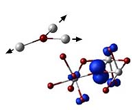
London UK (SPX) Oct 17, 2007 For the first time theoretical modeling has provided a glimpse into how promising dielectric materials are able to trap charges, something which may affect the performance of advanced electronic devices. This is revealed in a paper published on the 12th October in Physical Review Letters by researchers at the London Centre for Nanotechnology and SEMATECH, a company in Austin, Texas. Through the constant quest for miniaturization, transistors and all their components continue to decrease in size. A similar reduction has resulted in the thickness of a component material known as the gate dielectric - typically a thin layer of silicon dioxide, which has now been in use for decades. Unfortunately, as the thickness of the gate dielectric decreases, silicon dioxide begins to leak current, leading to unwieldy power consumption and reduced reliability. Scientists hope that this material can be replaced with others, known as high-dielectric constant (or high-k) dielectrics, which mitigate the leakage effects at these tiny scales. Metal oxides with high-k have attracted tremendous interest due to their application as novel materials in the latest generation of devices. The impetus for their practical introduction would be further helped if their ability to capture and trap charges and subsequent impact on instability of device performance was better understood. It has long been believed that these charge-trapping properties originate from structural imperfections in materials themselves. However, as is theoretically demonstrated in this publication, even if the structure of the high k dielectric material is perfect, the charges (either electrons or the absence of electrons - known as holes) may experience 'self trapping'. They do so by forming polarons - a polarizing interaction of an electron or hole with the perfect surrounding lattice. Professor Alexander Shluger of the London Centre for Nanotechnology and the Department of Physics and Astronomy at UCL says: "This creates an energy well which traps the charge, just like a deformation of a thin rubber film traps a billiard ball." The resulting prediction is that at low temperatures electrons and holes in these materials can move by hopping between trapping sites rather than propagating more conventionally as a wave. This can have important practical implications for the materials' electrical properties. In summary, this new understanding of the polaron formation properties of the transition metal oxides may open the way to suppressing undesirable characteristics in these materials. Community Email This Article Comment On This Article Related Links University College London London Centre for Nanotechnology Space Technology News - Applications and Research
 Columbus OH (SPX) Oct 16, 2007
Software under development at Ohio State University is helping scientists operate big-budget research instruments -- such as high-powered microscopes and telescopes -- over the Internet, more safely and efficiently than was possible before. The need for such remote operation is growing, and it's driven by the costs of doing research, explained Prasad Calyam, a doctoral student in electrical and computer engineering at Ohio State. |
|
| The content herein, unless otherwise known to be public domain, are Copyright 1995-2007 - SpaceDaily.AFP and UPI Wire Stories are copyright Agence France-Presse and United Press International. ESA Portal Reports are copyright European Space Agency. All NASA sourced material is public domain. Additional copyrights may apply in whole or part to other bona fide parties. Advertising does not imply endorsement,agreement or approval of any opinions, statements or information provided by SpaceDaily on any Web page published or hosted by SpaceDaily. Privacy Statement |