| . |  |
. |
| . | |
. |
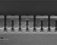
Troy NY (SPX) Jan 29, 2008 Researchers at Rensselaer Polytechnic Institute and Polyset Company have developed a new inexpensive, quick-drying polymer that could lead to dramatic cost savings and efficiency gains in semiconductor manufacturing and computer chip packaging. Along with allowing enhanced performance and cost savings for conventional photolithography processes, the new material, called polyset epoxy siloxane (PES), should also enable a new generation of lower-cost, on-chip nanoimprinting lithography technology, according to the researchers. "With this new material, chip manufacturers will be able to trim several steps from their production and packaging processes, and in turn realize a cost savings," said Toh-Ming Lu, the R.P. Baker Distinguished Professor of Physics at Rensselaer, who oversaw the study. "PES is cheaper and more reliable." Lu's research was published this week in the Journal of Vacuum Science and Technology B. The widely adopted technique of photolithography involves using a mix of light and chemicals to generate intricate micro- and nano-scale patterns on tiny areas of silicon. As part of the process, a thin polymer film - called a redistribution layer, and crucial to the effectiveness of device - is deposited onto the silicon wafer, in order to ease the signal propagation delay and to protect the chip from different environmental and mechanical factors. The new PES material developed by Lu's group and Polyset Company is one such thin polymer film, and it offers several advantages over the incumbent materials typically used in the semiconductor manufacturing industry. In addition, their new PES material can also be used as a thin polymer film for ultraviolet (UV) on-chip nanoimprinting lithography technology, which is still in the early phases of development. The consistency of using PES in conventional technology, and then continuing to use PES while academia and industry test and gradually migrate to the next generation of devices, should help ease the transition, Lu said. "Having the ability to use one material - our new PES - for both photolithography and imprint will be very attractive to manufacturers," Lu said. "At its core, our project is basic research, but it also has important industry implications. It's very exciting." Manufacturers today typically use benzocyclobutene and polyimide as polymers for redistribution layers, because of their low water absorption, thermal stability, low curing temperature, low thermal expansion, low dielectric constant, and low leakage current. Lu said PES offers significant advantages to these materials, particularly in the areas of cure temperature and water uptake. PES cures, or dries and hardens, at 165 degrees Celsius, about 35 percent cooler than the other two materials. The need for less heat should translate directly into lower overhead costs for manufacturers, Lu said. Another advantage of PES is its low water uptake rate of less than 0.2 percent, less than the other materials. Additionally, PES adheres well to copper and can easily be made less brittle if needed. All of these attributes make PES a promising candidate for redistribution layer application and UV imprint lithography. "The results demonstrate that PES is feasible to be used as UV-curable resist for both the redistribution application for electronic packaging and micro/nano imprint lithography," said Rensselaer Research Associate Pei-I Wang, co-author of the paper. Along with photolithography and on-chip nanoimprinting lithography, PES holds the potential for applications in other optical devices, flat-panel display, biotechnology devices, and microelectromechanical systems, Wang said. Community Email This Article Comment On This Article Related Links Rensselaer Polytechnic Institute Computer Chip Architecture, Technology and Manufacture Nano Technology News From SpaceMart.com
 Madison, Wis. (UPI) Jan 22, 2008
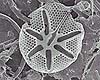
 U.S. scientists say the study of diatoms -- algae that encase themselves in patterned, glass-like shells -- might lead to an advance in computer chips. |
|
| The content herein, unless otherwise known to be public domain, are Copyright 1995-2007 - SpaceDaily.AFP and UPI Wire Stories are copyright Agence France-Presse and United Press International. ESA Portal Reports are copyright European Space Agency. All NASA sourced material is public domain. Additional copyrights may apply in whole or part to other bona fide parties. Advertising does not imply endorsement,agreement or approval of any opinions, statements or information provided by SpaceDaily on any Web page published or hosted by SpaceDaily. Privacy Statement |