| . |  |
. |
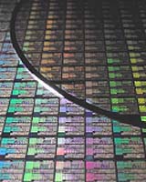
Aachen, Germany (SPX) Sep 06, 2005 A new nanotechnology tool that will dramatically cut the cost of leading-edge nano research at the sub-50nm scale has been developed by EU researchers. It could lead to Next Generation Lithography (NGL) technology. The commercially available first generation tool is low cost compared to sub-50nm alternatives. For example, electron beam lithography costs �2m per machine, whereas the Soft Ultraviolet (UV) Imprint machine developed by the IST-programme funded SOUVENIR project costs in its basic version well below �200,000. It will be used to produce novel and experimental nanotech devices in universities and research institutes. Later generations, however, could be used for small manufacturing runs. Further generations still could cause a fundamental shift in the semiconductor and nanotechnology industries. "In principle, this new technique has the potential to be used for mass manufacture by the semiconductor industry. One approach we use can already form patterns down to the 10nm scale," says Dr Markus Bender, researcher at German company, Applied Micro- and Optoelectronics (AMO), and coordinator of the SOUVENIR project.
The semiconductor industry's holy grail This is a big deal. Next Generation Lithography (NGL) is the holy grail of the semiconductor industry. It will allow rapid, large-scale manufacture of modern microchips at a sub-50nm scale. Industry giant Intel has spent 15 years and millions of dollars looking for it. A small team, but brilliant team of dedicated researchers in Europe may have found the solution in three years at a cost of �2,300,000. It will take a few years more research to know whether SOUVENIR's work will lead to viable NGL, but even with its first generation tool the SOUVENIR team have already generated remarkable results and a new product on the brink of commercialisation. Photolithography works by casting light through a mask to produce a pattern on a chemically-coated substrate. The light changes the chemical structure of the substrate. Depending on the type of photolithography, either the lit or shadowed chemical is washed away in the next step. In either case the result is a pattern etched into the substrate. With nanolithography the patterns are invisible to the naked eye and the vast majority of the world's microscopes. The result is the tiny circuits in semiconductor chips. The SOUVENIR project developed a new technique to create those patterns, one that is low cost and, comparatively, low tech. In a first step the substrate was coated with a low viscosity, UV-curable resist. The resist is simply a UV-sensitive chemical layered onto the substrate. They then used a soft polymer mould, called an elastomer, pressed against the resist-coated substrate, called imprinting, followed by the UV photopolymerisation, or curing, of the resist. This costs less than other photolithographic techniques. Because the mould is pressed against the resist, the system does not require the extremely expensive 'deep' UV light sources used in the semiconductor industry. These light sources can only work properly in a vacuum. Finally, the elastomer mould is considerably cheaper than those used in microchip manufacture. The result is a low-cost pattern process at the sub-50nm scale. However, the low cost comes at a price. Currently, the system is too slow and unproven to replace the current industrial photolithography processes. What's more, the elastomer moulds used in the SOUVENIR process at the moment need further improvements for high-resolution alignment processes, essential for mass manufacturing semiconductors. But ultimately it has the potential to become the next generation lithography. Thanks to research completed by the German government's Federal Ministry of Education and Research (BMBF), it is possible to use the same imprinting technique using a hard mould, based on quartz, which does have the required precision for semiconductor manufacture. "There a still problems with that particular technique," says Dr Bender. "The quartz approach only works with a substrate of one square inch, but we can use the elastomer mould on a six inch wafer," says Dr Bender. Furthermore, while quartz could address the precision issues the technique is currently too slow for large-scale semiconductor companies. But Dr Bender believes that with a commitment to research these hurdles could be overcome. "This is the first generation of the tool we developed and, with work, we can in principle get much better, faster and more scalable results," says Dr Bender. If he is right it could provide a viable alternative to the costly high-tech approach taken by Intel for Next Generation Lithography. The highly specialised light sources, mirrors and ultra-high vacuum used in Intel's Extreme Ultraviolet Light (EUVL) technique impose almost unconquerable and enormously expensive scaling constraints. After years and millions of dollars there is still no commercially viable EUVL system available. "I think there's the same potential with our technique as with the EUVL. UV imprinting is still an under-investigated area, and if it wasn't for the EU this research wouldn't get funded. Companies are not researching this field," says Dr Bender. "We are working in close cooperation with an Austrian company, Electronic Vision Group (EVG) to develop tools for the two approaches. I think next year we'll have a step and repeat tool for 300mm wafers on the market," says Dr Bender. This first generation tool is designed for small volume production, for example for chemical sensors and in biotechnology applications at small companies and research centres. Right now, small companies can't afford their own tools for sub-50nm nanotech devices. But ultimately, this research could change how the semiconductor industry works. "This is a totally new technique and we've got to prove that we can reliably reproduce the results. That's what we'll be doing now," says Dr Bender. Related Links More info on NextGen lithography SpaceDaily Search SpaceDaily Subscribe To SpaceDaily Express
 Santa Clara, California (AFP) Sep 01, 2005
Intel issued a scornful riposte Thursday to a lawsuit filed by Advanced Micro Devices that accuses the world's leading chip maker of bribing computer makers against using AMD processors. |
|
| The content herein, unless otherwise known to be public domain, are Copyright 1995-2006 - SpaceDaily.AFP and UPI Wire Stories are copyright Agence France-Presse and United Press International. ESA PortalReports are copyright European Space Agency. All NASA sourced material is public domain. Additionalcopyrights may apply in whole or part to other bona fide parties. Advertising does not imply endorsement,agreement or approval of any opinions, statements or information provided by SpaceDaily on any Web page published or hosted by SpaceDaily. Privacy Statement |