| . |  |
. |
| . | |
. |
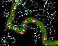
Exeter, UK (SPX) Jul 09, 2004 An ultrafine nanometre 'drill' could be used to make some of the tiniest lenses imaginable and may also allow scientists to harness light for use in optical computers of the future, thanks to research published today. Scientists from the UK and Spain describe in this week's Science Express (8 July) how artificial materials with tiny grooves and holes drilled into their surfaces could channel and focus light beams on a chip. When light hits the surface of a metal such as silver, as well as a reflection, another form of light is excited at the surface. This light, bound to the surface as a small mixture of light and electrons, is called a surface plasmon, its behaviour likened to waves on the surface of a 'sea' of electrons. For many years a curiosity, the properties of plasmons have only recently been fully explored. In their paper this week, the theorists show that holes perforating a surface can spoof the creation of these plasmons, and they suggest that the effect could be harnessed to channel light at tiny scales, overcoming one of the constraints facing designers of the first optical computer. "They aren't really plasmons but they behave like them," says Professor Sir John Pendry of Imperial College London and first author of the paper. "They capture light and lock them up in very tiny spaces." The holes, which may be just a few tens of nanometres wide, can be made using a special 'drill' called an ion-beam. A human hair is 100 times larger in diameter by comparison. This work suggests that engineered surface plasmons could be as simple as drilling holes in a perfectly conducting material. "It opens up a new dimension of design for the people looking to use surface plasmons to put light on a chip," says Sir John. By analogy with an electronic chip full of transistors, the most basic requirement is to join the bits together with wires. But in using light instead of electrons the challenge is how to replace the wires to move light around the chip. Optical fibre is not the answer as it is 50 microns wide and as big as the chip. "Instead of etching a path on a chip, now we could drill holes to make a path to control light on a chip," says Sir John. "The plasmons contain the same signals as the light exciting them and therefore can be used to transport information across the surface." "Alternatively we could send the plasmons across the surface in free flight, rather than in channels. We could drill holes to make lenses to focus it." Another use could be in shaping light. As light goes through holes in surfaces, smaller drilled grooves around the hole act to stop the light spreading out, focusing it instead, and in effect forming one of the tiniest lenses in the world at just a few microns wide. Research by Thomas Ebbesen and colleagues in 1998 at the University Louis Pasteur, Strasbourg, demonstrated a way of forcing light to go through tiny holes at the surface of a metal. By turning light into a surface plasmon then back again, they demonstrated that the effect worked, but only with the metals silver and gold. The theorists speculated that a material could be engineered that does not naturally have surface plasmons yet still has the same effect. "It turns out that if you take something completely inert, just by drilling holes you can make it behave as if it's got these surface excitations," says Sir John. "If you've got holes and you try to bounce light off the surface some light stays stuck in the holes, just as if it were stuck to the surface of silver in a surface plasmon." Surface plasmons were first described by Rufus Ritchie in the 1950s and subsequently applied by Ritchie and others to energy loss by the high voltage electrons in an electron microscope. Related Links The University of Exeter Imperial College London SpaceDaily Search SpaceDaily Subscribe To SpaceDaily Express
 Berkeley CA (SPX) Jul 08, 2004
Scientists at Lawrence Berkeley National Laboratory have found new ways of combining quantum dots and segmented nanorods into multiply branching forms and have applied new ways to calculate the electronic properties of these nanostructures, whose dimensions are measured in billionths of a meter. |
|
| The content herein, unless otherwise known to be public domain, are Copyright 1995-2006 - SpaceDaily.AFP and UPI Wire Stories are copyright Agence France-Presse and United Press International. ESA PortalReports are copyright European Space Agency. All NASA sourced material is public domain. Additionalcopyrights may apply in whole or part to other bona fide parties. Advertising does not imply endorsement,agreement or approval of any opinions, statements or information provided by SpaceDaily on any Web page published or hosted by SpaceDaily. Privacy Statement |