| . |  |
. |
| . | |
. |
|
by David L. Chandler fpr MIT News Boston MA (SPX) Mar 02, 2021
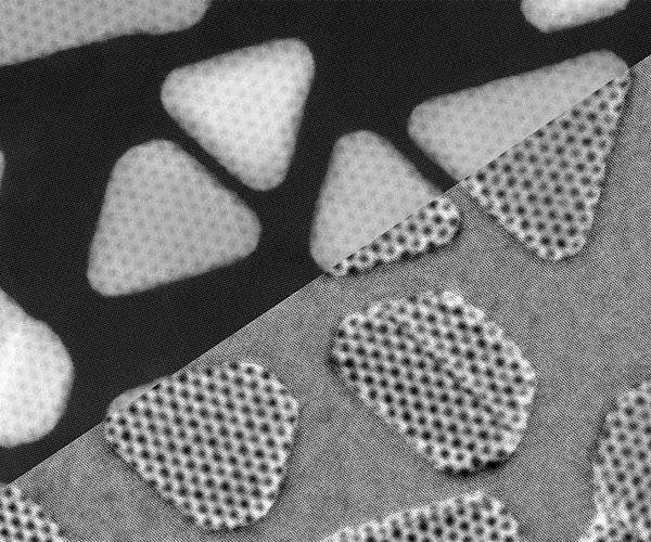
In recent years, engineers have found ways to modify the properties of some "two- dimensional" materials, which are just one or a few atoms thick, by stacking two layers together and rotating one slightly in relation to the other. This creates what are known as moire patterns, where tiny shifts in the alignment of atoms between the two sheets create larger-scale patterns. It also changes the way electrons move through the material, in potentially useful ways. But for practical applications, such two-dimensional materials must at some point connect with the ordinary world of 3D materials. An international team led by MIT researchers has now come up with a way of imaging what goes on at these interfaces, down to the level of individual atoms, and of correlating the moire patterns at the 2D-3D boundary with the resulting changes in the material's properties. The new findings are described in the journal Nature Communications, in a paper by MIT graduate students Kate Reidy and Georgios Varnavides, professors of materials science and engineering Frances Ross, Jim LeBeau, and Polina Anikeeva, and five others at MIT, Harvard University, and the University of Victoria in Canada. Pairs of two-dimensional materials such as graphene or hexagonal boron nitride can exhibit amazing variations in their behavior when the two sheets are just slightly twisted relative to each other. That causes the chicken-wire-like atomic lattices to form moire patterns, the kinds of odd bands and blobs that sometimes appear when taking a picture of a printed image, or through a window screen. In the case of 2D materials, "it seems like anything, every interesting materials property you can think of, you can somehow modulate or change by twisting the 2D materials with respect to each other," says Ross, who is the Ellen Swallow Richards Professor at MIT. While these 2D pairings have attracted scientific attention worldwide, she says, little has been known about what happens where 2D materials meet regular 3D solids. "What got us interested in this topic," Ross says, was "what happens when a 2D material and a 3D material are put together. Firstly, how do you measure the atomic positions at, and near, the interface? Secondly, what are the differences between a 3D-2D and a 2D-2D interface? And thirdly, how you might control it - is there a way to deliberately design the interfacial structure" to produce desired properties? Figuring out exactly what happens at such 2D-3D interfaces was a daunting challenge because electron microscopes produce an image of the sample in projection, and they're limited in their ability to extract depth information needed to analyze details of the interface structure. But the team figured out a set of algorithms that allowed them to extrapolate back from images of the sample, which look somewhat like a set of overlapping shadows, to figure out which configuration of stacked layers would yield that complex "shadow." The team made use of two unique transmission electron microscopes at MIT that enable a combination of capabilities that is unrivalled in the world. In one of these instruments, a microscope is connected directly to a fabrication system so that samples can be produced onsite by deposition processes and immediately fed straight into the imaging system. This is one of only a few such facilities worldwide, which use an ultrahigh vacuum system that prevents even the tiniest of impurities from contaminating the sample as the 2D-3D interface is being prepared. The second instrument is a scanning transmission electron microscope located in MIT's new research facility, MIT.nano. This microscope has outstanding stability for high-resolution imaging, as well as multiple imaging modes for collecting information about the sample. Unlike stacked 2D materials, whose orientations can be relatively easily changed by simply picking up one layer, twisting it slightly, and placing it down again, the bonds holding 3D materials together are much stronger, so the team had to develop new ways of obtaining aligned layers. To do this, they added the 3D material onto the 2D material in ultrahigh vacuum, choosing growth conditions where the layers self-assembled in a reproducible orientation with specific degrees of twist. "We had to grow a structure that was going to be aligned in a certain way," Reidy says. Having grown the materials, they then had to figure out how to reveal the atomic configurations and orientations of the different layers. A scanning transmission electron microscope actually produces more information than is apparent in a flat image; in fact, every point in the image contains details of the paths along which the electrons arrived and departed (the process of diffraction), as well as any energy that the electrons lost in the process. All these data can be separated out so that the information at all points in an image can be used to decode the actual solid structure. This process is only possible for state-of-the-art microscopes, such as that in MIT.nano, which generates a probe of electrons that is unusually narrow and precise. The researchers used a combination of techniques called 4D STEM and integrated differential phase contrast to achieve that process of extracting the full structure at the interface from the image. Then, Varnavides says, they asked, "Now that we can image the full structure at the interface, what does this mean for our understanding of the properties of this interface?" The researchers showed through modeling that electronic properties are expected to be modified in a way that can only be understood if the full structure of the interface is included in the physical theory. "What we found is that indeed this stacking, the way the atoms are stacked out-of-plane, does modulate the electronic and charge density properties," he says. Ross says the findings could help lead to improved kinds of junctions in some microchips, for example. "Every 2D material that's used in a device has to exist in the 3D world, and so it has to have a junction somehow with three-dimensional materials," she says. So, with this better understanding of those interfaces, and new ways to study them in action, "we're in good shape for making structures with desirable properties in a kind of planned rather than ad hoc way." "The present work opens a field by itself, allowing the application of this methodology to the growing research line of moire engineering, highly important in fields such as quantum physics or even in catalysis," says Jordi Arbiol of the Catalan Institute of Nanoscience and Nanotechnology in Spain, who was not associated with this work. "The methodology used has the potential to calculate from the acquired local diffraction patterns the modulation of the local electron momentum," he says, adding that "the methodology and research shown here has an outstanding future and high interest for the materials science community."
Research Report: "Direct imaging and electronic structure modulation of moire superlattices at the 2D/3D interface"

China's appetite for copper provides Chile with opportunity Santiago (AFP) Feb 25, 2021 With the price of copper reaching a 10-year high thanks in no small part to China's insatiable appetite, Chile, the world's leading producer, faces a "unique" opportunity, experts told AFP. Copper rose to $4.21 a pound on the London Metal Exchange on Wednesday, meaning it has doubled its price since March 2020. Now experts believe its price, spurred by demand from China, could beat all records in the coming weeks, surpassing its previous high of $4.60 in February 2011 and potentially rising abov ... read more
|
|||||||||||||
| The content herein, unless otherwise known to be public domain, are Copyright 1995-2026 - SpaceDaily. All websites are published in Australia and are solely subject to Australian law and governed by Fair Use principals for news reporting and research purposes. By using our websites you consent to cookie based advertising. If you do not agree with this then you must stop using the websites from May 25, 2018. Privacy Statement. Additional information can be found here at About Us. |
 del.icio.us
 Digg
Digg Reddit
 Google