| . |  |
. |
| . | |
. |
|
by Staff Writers Lausanne, Switzerland (SPX) Oct 04, 2016
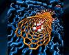
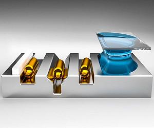
Whether it has to do with making pens or building space shuttles, the manufacturing process consists of creating components and then carefully assembling them. But when it comes to infinitely small structures, manipulating and assembling high-performance nanoparticles on a substrate is no mean feat. Researchers in EPFL's Laboratory of Microsystems, which is headed by Jurgen Brugger, have come up with a way to position hundreds of thousands of nanoparticles very precisely on a one centimeter square surface. The nanoparticles were placed within one nanometer - versus 10 to 20 nanometers using conventional methods - and oriented within one degree. Their work, which was published in Nature Nanotechnology, sets the stage for the development of nanometric devices such as optical detection equipment and biological sensors. "If we manage to place gold nanoparticles one nanometer apart, we could, for example, confine light to an extraordinary degree and detect or interact with individual molecules," said Valentin Flauraud, the lead author. For their study, the researchers used gold nanoparticles that were grown chemically in a liquid. "These nanoparticles exhibit better properties than those produced through evaporation or etching, but it is more difficult to manipulate them, because they are suspended in a liquid," said Flauraud. Their technique consists of taking a drop of liquid full of nanoparticles and heating it so that the nanoparticles cluster in a given spot. This drop is then dragged across a substrate with nanometric barriers and holes. When the nanoparticles encounter these obstacles, they detach from the liquid and are captured by the holes. "It's a little like playing miniature golf," said the researcher. Each trap is designed to orient a nanoparticle in a specific way. "The challenge was to figure out how the liquid, the particles and the substrate interact at the nanometric scale so we could trap the nanoparticles effectively," said Massimo Mastrangeli, the second author and now a researcher at the Max Planck Institute for Intelligent Systems in Stuttgart. To show how well their method works, the researchers took on several challenges. First, they tested the optical properties of their system with a powerful transmission electron microscope in EPFL's Interdisciplinary Center for Electron Microscopy (CIME). They then showed that their technique could be used to produce geometrically complex structures by writing out the alphabet with nanoparticles - the smallest segment display in the world. "All of this work was conducted at EPFL and is the result of strong synergies between the various technical platforms and the labs," said Professor Brugger. "It's an excellent example of how top-down and bottom-up methods can be combined, opening the door to numerous unexplored fields of nanotechnology."
Related Links Ecole Polytechnique Federale de Lausanne Nano Technology News From SpaceMart.com Computer Chip Architecture, Technology and Manufacture
|
|||||||||||||
| The content herein, unless otherwise known to be public domain, are Copyright 1995-2026 - SpaceDaily. All websites are published in Australia and are solely subject to Australian law and governed by Fair Use principals for news reporting and research purposes. By using our websites you consent to cookie based advertising. If you do not agree with this then you must stop using the websites from May 25, 2018. Privacy Statement. Additional information can be found here at About Us. |
 del.icio.us
 Digg
Digg Reddit
 Google