| . |  |
. |
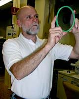
for Air Force Research Lab, Propulsion Directorate Wright-Patterson AFB OH (AFNS) May 15, 2006 Dr. James Scofield, an electrical engineer with the Air Force Research Laboratory Propulsion Directorate's Electrical Technology and Plasma Physics Branch, has received the 2006 Federal Laboratory Consortium Award for Excellence in Technology Transfer for pioneering the new and improved silicon carbide (SiC) Schottky diodes. Development of a new breed of semiconducting material is transforming the operation of electronic devices. The development is responsible for an increase in system efficiency and operational reliability in power electronic circuit applications. Schottky diodes are high-speed rectifying devices in an electronic circuit. Until recently, they were exclusively fabricated using silicon, and were limited to applications of 200 volts or less due to fundamental material properties. Because the breakdown field strength of SiC is ten times that of Si, Schottky diodes made with SiC easily achieve device ratings in the 600-1200 volt/ 1-100 amp range, with on-resistance characteristics similar to the lower voltage Si parts. Silicon carbide, a member of the so-called "wide bandgap" class of semiconducting materials, provides the diodes with many characteristics that are desirable in Air Force power applications. SiC enables higher switching speeds, higher temperature operation, reduced energy losses, resistance to ionizing radiation, and electronics cooling system size and weight reduction. Scofield developed SiC plasma processing and thermal annealing techniques that are used to fabricate silicon carbide power electronic devices. He was responsible for the technology transfer and collaboration with Mississippi State University that contributed to the establishment of a viable manufacturer of SiC power devices, SemiSouth Laboratories. At the same time, he initiated a Dual Use Science and Technology agreement with Cree, Inc., which led to the development and commercialization of SiC Schottky power devices. The fabrication process used for these commercial parts utilizes the implantation anneal process pioneered by Scofield, and is responsible for significant improvements to production yields, device reliability, and a reduction in manufacturing cost. The FY05 revenue from these commercial SiC Schottky diodes exceeded $10 million and significant growth is projected for fiscal year 2006 as the technology is increasingly embraced by component developers and design engineers. The replacement of silicon with silicon carbide diodes can significantly improve the overall operational efficiency of power systems. SiC material enables faster switching speeds, which allows the design of higher frequency power converters and inverters, which in-turn allows a reduction in the size and weight of passive capacitor and inductor circuit elements increasing power density. It is also capable of functioning at temperatures of up to 300� C, compared to the Si operational limit of 150� C. "The road to a practical semiconductor material beyond silicon has been long and difficult ,"said Dr. Bill Borger, director of Air Force Research Laboratory's Propulsion Directorate. "Efforts date back to the late 1960s when researchers attempted to make high temperature alternators for high Mach aircraft. Diodes based on Silicon Carbide were formulated then that enabled aircraft alternators to operate at extremely high temperatures, exceeding 300 degrees. However, these early devices were neither reliable nor cost effective. Not until Scofied's work can we point to Silicon Carbide diodes as marketable devices." SiC Schottky diodes have a high blocking voltage rating of up to 1200 volts commercially, with a practical potential of up to 3000 volts for ultra-high power density applications. "Because of their faster switching speed, high temperature capability, and efficiency advantages, SiC Schottky devices can now offer high performance solutions for a wide range of power system applications requiring improved performance and increased power density," stated Scofield. "Applications include industrial motor drives, power factor correction, energy efficient kitchen appliances, power supplies, and a host of other commercial power applications in addition to the harsh environment Defense weapon system applications," he noted. "With rapidly increasing energy costs, and the push toward hybrid and electric vehicles, SiC will eventually power the traction drive motors in automotive applications. "This application demands a high temperature capable power technology as the available cooling from radiator loop liquid is in the 90 to 110oC range, which is pushing the limit of Si IGBT traction drive inverter technology from a reliability standpoint," Scofield explained. "Power switch maturation, volume availability, and cost remain issues for this application, but a rapidly improving SiC technology and commercial demand will eliminate these obstacles." The manufacturing of SiC Schottky Diodes has proven beneficial to both military and commercial applications. The Air Force is developing inverters, converters and motor drives with the new SiC semiconducting technology. The Air Force More Electric Aircraft, or MEA, concept is dependent upon theses and other emerging SiC power devices. This concept involves replacing all hydraulic, pneumatic, and mechanical powered systems with electronic functionality to improve the reliability, maintainability, and life cycle cost of aircraft. Continued use of SiC Schottky Diodes and similar high efficiency power technologies will lead to increased electrical performance, which will help meet the increasing power demands of a boundlessly growing electronic world. Related Links in system efficiency and operational reliability in power electronic circuit applications.
 Atlanta GA (SPX) Apr 26, 2006
Using a combination of experimental data and simulations, researchers have identified key parameters that predict the outcome of nanoimprint lithography, a fabrication technique that offers an alternative to traditional lithography in patterning integrated circuits and other small-scale structures into polymers. |
|
| The content herein, unless otherwise known to be public domain, are Copyright 1995-2006 - SpaceDaily.AFP and UPI Wire Stories are copyright Agence France-Presse and United Press International. ESA PortalReports are copyright European Space Agency. All NASA sourced material is public domain. Additionalcopyrights may apply in whole or part to other bona fide parties. Advertising does not imply endorsement,agreement or approval of any opinions, statements or information provided by SpaceDaily on any Web page published or hosted by SpaceDaily. Privacy Statement |