| . |  |
. |
| . | |
. |
|
by Staff Writers Urbana IL (SPX) Jan 20, 2017
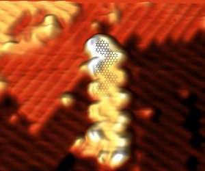
Silicon crystals are the semiconductors most commonly used to make transistors, which are critical electronic components used to carry out logic operations in computing. However, as faster and more powerful processors are created, silicon has reached a performance limit: the faster it conducts electricity, the hotter it gets, leading to overheating. Graphene, made of a single-atom-thick sheet of carbon, stays much cooler and can conduct much faster, but it must be into smaller pieces, called nanoribbons, in order to act as a semiconductor. Despite much progress in the fabrication and characterization of nanoribbons, cleanly transferring them onto surfaces used for chip manufacturing has been a significant challenge. A recent study conducted by researchers at the Beckman Institute for Advanced Science and Technology at the University of Illinois and the Department of Chemistry at the University of Nebraska-Lincoln has demonstrated the first important step toward integrating atomically precise graphene nanoribbons (APGNRs) onto nonmetallic substrates. The paper, "Solution-Synthesized Chevron Graphene Nanoribbons Exfoliated onto H:Si(100)," was published in Nano Letters. Graphene nanoribbons measure only several nanometers across, beyond the limits of conventional chip top-down patterning used in chip manufacturing. As a result, when carved from larger pieces of graphene by various nanofabrication approaches, graphene nanoribbons are neither uniform nor narrow enough to exhibit the desired semiconductor properties. "When you're going from the top-down, it's very hard to get control over the width. It turns out that if the width modulates by just an atom or two, the properties change significantly," said Adrian Radocea, a doctoral student in Beckman's Nanoelectronics and Nanomaterials Group. As a result, the nanoribbons must be made from "the bottom up," from smaller molecules to create atomically precise nanoribbons with highly uniform electronic properties. "It's like molecular building blocks: kind of like snapping Legos together to building something," said Radocea. "They lock in place, and you end up with the exact control over the ribbon width." The "bottom-up" approach was first shown for graphene nanoribbons by Cai et al. in a 2010 Nature paper demonstrating the growth of atomically precise graphene nanoribbons on metallic substrates. In 2014, the research group of Alexander Sinitskii at the University of Nebraska-Lincoln developed an alternative approach for making atomically precise graphene nanoribbons in solution. "The previously demonstrated synthesis on metallic substrates yields graphene nanoribbons of very high quality, but their number is rather small, as the growth it limited to the precious metal's surface," said Sinitskii, associate professor of chemistry at University of Nebraska-Lincoln and an author of the study. "It is difficult to scale this synthesis up. In contrast, when nanoribbons are synthesized in the unrestricted three-dimensional solution environment, they can be produced in large quantities." The difficulty in cleanly transferring nanoribbons stems from the high sensitivity to environmental contaminants. Both solution-synthesized and surface-grown nanoribbons are exposed to chemicals during the transfer process that can affect the performance of graphene nanoribbon devices. To overcome this challenge, the interdisciplinary team used a dry transfer in an ultra-high vacuum environment. A fiberglass applicator coated in graphene nanoribbon powder was heated to remove contaminants and solvent residue and then pressed onto a freshly prepared hydrogen-passivated silicon surface. The nanoribbons were studied in great detail with ultra-high vacuum scanning tunneling microscope developed by Joseph Lyding, professor of electrical and computer engineering at Illinois and an author of the study. The researchers obtained atomic-scale images and electronic measurements of the graphene nanoribbons that were critical for confirming their electronic properties and understanding the influence of the substrate. Computational expertise available at Beckman, Radocea explained, was instrumental in understanding the experimental results. "I was still collecting more data trying to figure out what was going on. Once the modeling results came in and we started looking at the data differently, it all made sense." Members of Beckman's Computational Multiscale Nanosystems Group, Tao Sun, a doctoral student, and Narayana Aluru, professor of mechanical science and engineering, provided expertise in computational modeling via density functional theory to investigate the properties of the nanoribbons. "Density functional theory calculations provided a deeper understanding of the electronic properties of the integrated system and the interactions between graphene nanoribbons and the silicon substrate," said Sun. "It was exciting that the computational results could help explain and confirm the experimental results and provided a coherent story." "Atomically precise graphene nanoribbons (APGNRs) are serious candidates for the post-silicon era when conventional silicon transistor scaling fails," said Lyding. "This demonstrates the first important step toward integrating APGNRs with technologically relevant silicon substrates." "I find the project very exciting because you are building things with atomic level control, so you try to put every atom exactly where you want it to go," said Radocea. "There aren't many materials out there where you can say you have that ability. Nanoribbons are exciting because there is a real need and a real application."
Related Links Beckman Institute for Advanced Science and Technology Nano Technology News From SpaceMart.com Computer Chip Architecture, Technology and Manufacture
|
|||||||||||||
| The content herein, unless otherwise known to be public domain, are Copyright 1995-2026 - SpaceDaily. All websites are published in Australia and are solely subject to Australian law and governed by Fair Use principals for news reporting and research purposes. By using our websites you consent to cookie based advertising. If you do not agree with this then you must stop using the websites from May 25, 2018. Privacy Statement. Additional information can be found here at About Us. |
 del.icio.us
 Digg
Digg Reddit
 Google