| . |  |
. |
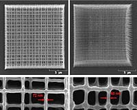
Atlanta GA (SPX) Mar 28, 2007 Producing three-dimensional polymer line structures as small as 65 nanometers wide just became easier with new two-photon absorbing molecules that are sensitive to laser light at short wavelengths, allowing researchers to create them without highly sophisticated fabrication methods. Fabricating such small features normally requires expensive electron beam or extreme ultraviolet lithography equipment. However, using a technique called 3D multi-photon lithography simplifies the process and reduces the cost. The technique could compete with existing processes for fabricating nanoscale electronic, photonic and microfluidic devices. "Being able to obtain line widths down to 65 nanometers, which is substantially below prior published work of 100 nanometers, opens up new applications for multi-photon lithography," said Joseph Perry, a professor in the Georgia Tech School of Chemistry and Biochemistry and the Center for Organic Photonics and Electronics. The technique scans a laser beam across a substrate coated with a polymer resin containing a unique dye to create a desired hardened polymer structure. The laser writing process takes advantage of the fact that the chemical reaction of cross-linking occurs only where molecules have absorbed two photons of light. Since the rate of two-photon absorption drops off rapidly with distance from the laser's focal point, only molecules at the focal point receive enough light to absorb two photons. The fabrication method and dye were described in the March 19 issue of Optics Express. The research was supported by the Office of Naval Research APEX Consortium and the National Science Foundation, through the Science and Technology Center for Materials and Devices for Information Technology Research. Seth Marder and Stephen Barlow, also researchers in the School of Chemistry and Biochemistry and the Center for Organic Photonics and Electronics, synthesized the unique molecule called DAPB, 4,4'-bis(di-n-butylamino)biphenyl, to initiate the chemical reaction leading to the hardening of the polymers when exposed to laser light. "We needed a dye with good two-photon absorption at a wavelength of 520 nanometers, so we tried DAPB," explained Perry. "DAPB proved to be very effective in this kind of lithography." The molecule developed by Marder and Barlow is about ten times more efficient at absorbing light by two photon absorption than commercial ultraviolet photoactive materials. That efficiency allowed Perry and graduate students Wojciech Haske and Vincent Chen, research scientist Joel Hales and postdoctoral associate Wenting Dong to create 3D patterns with nanoscale lines at light intensities low enough to avoid damaging the polymers. For the experiments, a film of the polymer resin containing DAPB was formed. When the film was exposed to the focused laser, DAPB was excited and triggered cross-linking, leaving the insoluble scanned structure on the surface of a substrate when placed in a developer solution. Since Perry controls where the Ti: Sapphire pulsed laser scans with a computer program, the polymers can be cross-linked in any pattern including 3D stacks of straight lines that are connected and sturdy. The laser beam is turned on to expose lines of polymer and off when no line should be drawn. Conventional lithography involves creating a specific pattern on a mask for each new layer and exposing each layer to light and developing it. With this new technique, three-dimensional layered nanostructures can be created simply by having a computer program scan a different pattern for each layer. Mask templates become unnecessary and the coating, exposing and developing processes only have to be conducted once. "We can create essentially any pattern we want. For this work, some of the patterns look like walls or lines suspended across walls and some are like a tall stack of crisscrossed lines," noted Perry. Perry and Marder co-founded a company in 2003 called Focal Point Microsystems that is working to commercialize this fabrication technology. "We can write very small lines and create stacked-up grids of lines called photonic crystals," explained Perry. "This work shows that we can fabricate functional photonic micro-devices with tailored transmission capabilities." It takes only 10 minutes to create a 20 micron by 20 micron structure with 30 layers, Perry added. Perry envisions using this technology to create compact micro-spectrometers on a chip for use in telecommunications and sensors. It may also be used as a compact way to separate the multiple wavelengths traveling through a fiber optic cable. This type of simple, table-top technology may also be useful to fabricate customized types of circuits with many layers, which would be extremely expensive with standard methods because each layer would require a special mask. "With the combination of the right molecule and short wavelength light, we've demonstrated that we can obtain nanoscale features. We're at 65 nanometers now and we're still trying to go smaller," said Perry. Email This Article
Related Links
 Chicago IL (SPX) Mar 28, 2007
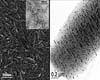
Appropriating cellulose fibers from cotton and crystallizing them, scientists at Pacific Northwest National Laboratory have grown never-before-seen configurations of metal crystals that show promise as components in biosensors, biological imaging, drug delivery and catalytic converters. |
|
| The content herein, unless otherwise known to be public domain, are Copyright 1995-2006 - SpaceDaily.AFP and UPI Wire Stories are copyright Agence France-Presse and United Press International. ESA PortalReports are copyright European Space Agency. All NASA sourced material is public domain. Additionalcopyrights may apply in whole or part to other bona fide parties. Advertising does not imply endorsement,agreement or approval of any opinions, statements or information provided by SpaceDaily on any Web page published or hosted by SpaceDaily. Privacy Statement |