| . |  |
. |
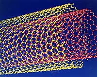
The Weizmann Institute of Science recently announced that a research group headed by Dr. Ernesto Joselevich has developed a new approach to create patterns of carbon nanotubes by formation along atomic steps on sapphire surfaces. Carbon nanotubes are excellent candidates for the production of nanoelectronic circuits, but their assembly into ordered arrays remains a major obstacle toward this application. The team was initially researching in a different direction: they were trying to give carbon nanotubes (structures reminiscent of rolled-up sheets of graphite) a preferred orientation on a wafer by applying an electrical field as the tubes were being formed. This works very well with silicon dioxide wafers. On a sapphire support (sapphire is a form of aluminum oxide), on the other hand, it didn't work: the nanotubes were beautifully arranged in parallel, but with an orientation that was completely independent of the electrical field � even when no field was applied at all. Closer examination of the sapphire surface solved the mystery: commercial sapphire wafers are generally not cut exactly along the plane of the crystal. Their surface is thus not completely smooth; instead, it has parallel steps � of atomic dimensions � between the different planes of the crystal. The nanotubes wind up lying along these steps. The researchers explain it like this: the nanotubes form from a catalyst of iron nanoparticles and are attracted to a local field created by the steps. It is clear that these iron particles don't like "climbing stairs;" instead, they "glide" along the inner edge of the step, as though on a track. Thus they remain continuously in contact with two surfaces, rather than just one, which seems to stabilize the catalyst. Just as an airplane leaves behind a condensation trail, the iron particles leave the newly formed nanotubes lying along their "tracks." The nanotubes even follow kinks in the steps, which are caused by defects in the crystal. This results in either straight or zigzag-shaped tubes, which are expected to have particularly interesting electronic properties. "The orientation and form of the atomic steps on a crystal surface can be controlled by the cutting process, and defects can be created artificially," says Joselevich. "It should thus be possible to produce different nanowire arrangements in a controlled fashion." Related Links Weizmann Institute SpaceDaily Search SpaceDaily Subscribe To SpaceDaily Express  New York (UPI) Dec 27, 2004
The global market for nanosensors - sensors with components only billionths of a meter in size - is predicted to reach only a modest $185 million or so in 2005, but forecasters told United Press International's Nano World they expect it to skyrocket to $2.7 billion in 2008 and $17.2 billion in 2012, writes Charles Choi.
|
| ||||||||||
| The content herein, unless otherwise known to be public domain, are Copyright 1995-2016 - Space Media Network. All websites are published in Australia and are solely subject to Australian law and governed by Fair Use principals for news reporting and research purposes. AFP, UPI and IANS news wire stories are copyright Agence France-Presse, United Press International and Indo-Asia News Service. ESA news reports are copyright European Space Agency. All NASA sourced material is public domain. Additional copyrights may apply in whole or part to other bona fide parties. Advertising does not imply endorsement, agreement or approval of any opinions, statements or information provided by Space Media Network on any Web page published or hosted by Space Media Network. Privacy Statement All images and articles appearing on Space Media Network have been edited or digitally altered in some way. Any requests to remove copyright material will be acted upon in a timely and appropriate manner. Any attempt to extort money from Space Media Network will be ignored and reported to Australian Law Enforcement Agencies as a potential case of financial fraud involving the use of a telephonic carriage device or postal service. |