|
|
| . |  |
. |
|
|
by Staff Writers Austin TX (SPX) May 12, 2009
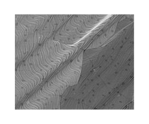
The creation of large-area graphene using copper may enable the manufacture of new graphene-based devices that meet the scaling requirements of the semiconductor industry, leading to faster computers and electronics, according to a team of scientists and engineers at The University of Texas at Austin. Their work titled "Large-Area Synthesis of High-Quality and Uniform Graphene Films on Copper Foils" was published online in Science Express in advance of its print publication in the journal Science. "Graphene could lead to faster computers that use less power, and to other sorts of devices for communications such as very high-frequency (radio-frequency-millimeter wave) devices," said Professor and physical chemist Rod Ruoff, one of the corresponding authors on the Science article. "Graphene might also find use as optically transparent and electrically conductive films for image display technology and for use in solar photovoltaic electrical power generation." Graphene, an atom-thick layer of carbon atoms bonded to one another in a "chickenwire" arrangement of hexagons, holds great potential for nanoelectronics, including memory, logic, analog, opto-electronic devices and potentially many others. It also shows promise for electrical energy storage for supercapacitors and batteries, for use in composites, for thermal management, in chemical-biological sensing and as a new sensing material for ultra-sensitive pressure sensors. "There is a critical need to synthesize graphene on silicon wafers with methods that are compatible with the existing semiconductor industry processes," Ruoff said. "Doing so will enable nanoelectronic circuits to be made with the exceptional efficiencies that the semiconductor industry is well known for." Graphene can show very high electron- and hole-mobility; as a result, the switching speed of nanoelectronic devices based on graphene can in principle be extremely high. Also, graphene is "flat" when placed on a substrate (or base material) such as a silicon wafer and, thus, is compatible with the wafer-processing approaches of the semiconductor industry. The exceptional mechanical properties of graphene may also enable it to be used as a membrane material in nanoelectromechanical systems, as a sensitive pressure sensor and as a detector for chemical or biological molecules or cells. The university researchers, including post-doctoral fellow Xuesong Li, and Luigi Colombo, a TI Fellow from Texas Instruments, Inc., grew graphene on copper foils whose area is limited only by the furnace used. They demonstrated for the first time that centimeter-square areas could be covered almost entirely with mono-layer graphene, with a small percentage (less than five percent) of the area being bi-layer or tri-layer flakes. The team then created dual-gated field effect transistors with the top gate electrically isolated from the graphene by a very thin layer of alumina, to determine the carrier mobility. The devices showed that the mobility, a key metric for electronic devices, is significantly higher than that of silicon, the principal semiconductor of most electronic devices, and comparable to natural graphite. "We used chemical-vapor deposition from a mixture of methane and hydrogen to grow graphene on the copper foils," said Ruoff. "The solubility of carbon in copper being very low, and the ability to achieve large grain size in the polycrystalline copper substrate are appealing factors for its use as a substrate --along with the fact that the semiconductor industry has extensive experience with the use of thin copper films on silicon wafers. By using a variety of characterization methods we were able to conclude that growth on copper shows significant promise as a potential path for high quality graphene on 300-millimeter silicon wafers." The university's effort was funded in part by the state of Texas, the South West Academy for Nanoelectronics (SWAN) and the DARPA CERA Center. Electrical and computer engineering Professor Sanjay Banerjee, a co-author of the Science paper, directs both SWAN and the DARPA Center. "By having a materials scientist of Colombo's caliber with such extensive knowledge about all aspects of semiconductor processing and now co-developing the materials science of graphene with us, I think our team exemplifies what collaboration between industrial scientists and engineers with university personnel can be," said Ruoff, who holds the Cockrell Family Regents Chair No.7. "This industry-university collaboration supports both the understanding of the fundamental science as well its application."
Related Links University of Texas at Austin Powering The World in the 21st Century at Energy-Daily.com
|
|
| The content herein, unless otherwise known to be public domain, are Copyright 1995-2014 - Space Media Network. AFP, UPI and IANS news wire stories are copyright Agence France-Presse, United Press International and Indo-Asia News Service. ESA Portal Reports are copyright European Space Agency. All NASA sourced material is public domain. Additional copyrights may apply in whole or part to other bona fide parties. Advertising does not imply endorsement,agreement or approval of any opinions, statements or information provided by Space Media Network on any Web page published or hosted by Space Media Network. Privacy Statement |
 del.icio.us
 Digg
Digg Reddit
 Google