Subscribe free to our newsletters via your
. 24/7 Space News .


CHIP TECH
Germanium made compatible
Maja Schaffner for ETH Zurich
Zurich, Switzerland (SPX) Apr 23, 2013


Light emitting bridges of germanium can be used for communication between microprocessors. (Graphic: Hans Sigg, PSI).

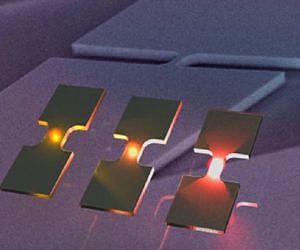
Researchers from ETH Zurich, the Paul Scherrer Institute (PSI) and the Politecnico di Milano have jointly developed a manufacturing technique to render the semiconductor germanium laser-compatible through high tensile strain. In their paper recently published in Nature Photonics, they reveal how they can generate the necessary tensile strain efficiently.

The scientists demonstrate that they can use their method to effectively alter the optical properties of germanium, which is unsuitable for lasers as such: "With a strain of three per cent, the material emits around twenty-five times more photons than in a relaxed state," explains Martin Suess, a doctoral student at the Laboratory for Nanometallurgy headed by Ralph Spolenak and the EMEZ at ETH Zurich.

"That's enough to build lasers with," adds his colleague Richard Geiger, a doctoral student at the Laboratory for Micro- and Nanotechnology at the PSI and the Institute for Quantum Electronics at ETH Zurich under Jerome Faist.

High tension through microbridges
In order to bring the germanium into a laser-compatible, stretched form with the new method, the researchers use the slight tension generated in germanium when it evaporates on silicon, strengthening this prestrain with so-called microbridges: they score exposed germanium strips, which remain attached to the silicon layer at both ends, in the middle on both sides.

The two halves of the strip thus remain connected solely by an extremely narrow bridge, which is precisely where, for physical reasons, the strain of the germanium grows so intense that it becomes laser-compatible.

"The tensile strain exerted on the germanium is comparable to the force exerted on a pencil as two lorries pull upon it in opposite directions," says Hans Sigg, the project manager at the PSI, explaining the feat on a micrometre scale in everyday proportions. The material properties change because the individual atoms move apart a little through the expansion of the material, which enables the electrons to reach energy levels that are favourable for the generation of light particles, so-called photons.

Germanium laser for the computer of the future
The interdisciplinary research team's method could increase the performance of future computer generations considerably. After all, in order to improve computer performance, computer chips have constantly been made smaller and more densely packed. However, this approach will eventually hit a brick wall in the foreseeable future.

"In order to increase performance and speed further, the individual components need to be linked more closely and communicate with each other more efficiently," explains Suess. This requires new transmission paths that are faster than today, where the signals are still transmitted via electricity and copper cables.

"The way to go in future is light," says Geiger.
In order to be able to use this to transfer data, however, first of all light sources are needed that are so small as to fit onto a chip and react well to silicon, the base material of all computer chips. Silicon itself is not suitable for the construction of laser light, which is also the reason why it is so important for the researchers to make germanium laser-compatible: "Germanium is perfectly compatible with silicon and already used in the computer industry in the production of silicon chips," explains Geiger.

If it is possible to build tiny lasers out of germanium using the new method, a system change is within reach. "We're on the right track," says Suess. The international team of researchers is currently in the process of actually constructing a germanium laser with the new method.

Suess MJ, Geiger R, Minamisawa RA, Schiefler G, Frigerio J, Chrastina D, Isella G, Spolenak R, Faist J and Sigg H: Analysis of enhanced light emission from highly strained germanium microbridges. Nature Photonics. 2013. Published online: 14 April 2013 doi:10.1038/nphoton.2013.67.

.


Related Links
ETH Zurich
Computer Chip Architecture, Technology and Manufacture
Nano Technology News From SpaceMart.com


Comment on this article via your Facebook, Yahoo, AOL, Hotmail login.

Share this article via these popular social media networks
del.icio.usdel.icio.us DiggDigg RedditReddit GoogleGoogle


CHIP TECH
Revolutionary new device joins world of smart electronics
Exeter UK (SPX) Apr 23, 2013
Smart electronics are taking the world by storm. From techno-textiles to transparent electronic displays, the world of intelligent technology is growing fast and a revolutionary new device has just been added to its ranks. Researchers at the University of Exeter have developed a new photoelectric device that is both flexible and transparent. The device, described in a paper in the journal ... read more


CHIP TECH
Characterizing The Lunar Radiation Environment

Russia rekindles Moon exploration program, intends setting up first human outposts there

Pre-existing mineralogy may survive lunar impacts

Lunar cycle determines hunting behaviour of nocturnal gulls

CHIP TECH
Dutch reality show seeks one-way astronauts for Mars

Accurate pointing by Curiosity

NASA Mars Orbiter Images May Show 1971 Soviet Lander

Opportunity is in position for solar conjunction at 'Cape York' on the rim of Endeavour Crater

CHIP TECH
Google's Brin keeps spotlight on future technologies

Mysterious water on Jupiter came from comet smash

What makes a good astronaut?

NASA urged to preserve funding for planetary science missions

CHIP TECH
Yuanwang III, VI depart for space-tracking missions

Shenzhou's Shadow Crew

Shenzhou 10 sent to launch site

China's Next Women Astronauts

CHIP TECH
ISS Communications Test Bed Checks Out; Experiments Begin

Spacewalkers Deploy Plasma Experiment, Install Navigational Aid

The New and Improved ISS Facilities Brochure

Full tank, please For ATV Einstein

CHIP TECH
Vega's three-satellite payload is integrated and ready for launch

NASA Seeks Innovative Suborbital Flight Technology Proposals

Stephane Israel named Chairman and CEO of Arianespace

Launch pad problem scrubs launch of Antares rocket for NASA

CHIP TECH
Mysterious Hot Spots Observed In A Cool Red Supergiant

Orbital Selected By NASA for TESS Astrophysics Satellite

Star-and Planet-Forming Regions May Hold Key to Life's Chirality

Kepler Discovers Its Smallest Habitable Zone Planets

CHIP TECH
Space debris problem now urgent - scientists

Nothing Bugs These NASA Aeronautical Researchers

US eases export rules on aerospace parts

MEADS Low Frequency Sensor Cues Multifunction Fire Control Radar in Test


The content herein, unless otherwise known to be public domain, are Copyright 1995-2014 - Space Media Network. AFP, UPI and IANS news wire stories are copyright Agence France-Presse, United Press International and Indo-Asia News Service. ESA Portal Reports are copyright European Space Agency. All NASA sourced material is public domain. Additional copyrights may apply in whole or part to other bona fide parties. Advertising does not imply endorsement,agreement or approval of any opinions, statements or information provided by Space Media Network on any Web page published or hosted by Space Media Network. Privacy Statement