| . |  |
. |
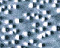
Scientists at Lawrence Berkeley National Laboratory have found new ways of combining quantum dots and segmented nanorods into multiply branching forms and have applied new ways to calculate the electronic properties of these nanostructures, whose dimensions are measured in billionths of a meter. The remarkable new branched structures are described in the July 8 issue of Nature by researchers in the laboratory of Paul Alivisatos, director of Berkeley Lab's Materials Sciences Division and professor of chemistry at the University of California at Berkeley, and by members of the Scientific Computing Group in Berkeley Lab's Computational Research Division, in affiliation with the Department of Energy's National Energy Research Scientific Computing Center (NERSC) based here. The ability to independently tune the separate components of the nanostructures with unprecedented accuracy, and to calculate the electronic interactions of their branches in three dimensions, will enable researchers to create electronic devices tailored to a variety of uses. The structures can be chemically manufactured in large quantities, for potential applications ranging from quantum computing to artificial photosynthesis.
Building branched nanostructures Steve Hughes, also a graduate student on the project, explains that "between no branching and excessive branching there's a fine point where the tetrapods form nicely." At a high concentration of cadmium and tellurium in suspension the atoms crystallize into the cubic zincblende structure, whereas at lower concentrations the compound grows in the hexagonal wurtzite structure. The two kinds of crystal are otherwise similar, with each atom bonding to four others. Says Milliron, "It occurred to us that for electronic purposes we might be able to make branching structures from more than one kind of material � theoretically you could use anything with the two crystal phases. Once you have two materials, the branching possibilities increase enormously." The Alivisatos group, having long experience with cadmium compounds, used suspensions of cadmium, selenium, tellurium, sulfur, and other constituents. When these are assembled from liquid solution, crystals of different cadmium compounds are formed. "Sure enough, the very first time I tried it, I got branches," says Milliron. A given structure begins with a quantum dot, described by post-doctoral fellow Yi Cui as "a conglomeration of a few hundreds or thousands of atoms in which it's possible to control a single electron." The dot is then made to sprout four arms made of the same or a different compound so that, says Cui, "Now you've effectively got four quantum rods coupled electronically with the central quantum dot. These coupled quantum systems might be useful in quantum computation." The arms of such a tetrapod can be lengthened into nanorods containing segments of different compounds. Nanorods, whether or not they are the arms of tetrapods, can be induced to branch into separate rods of the same or a different compound. New chemical procedures allow the branch points to be specified at will and different materials to be grown selectively on the ends of the nanorods. Calculating the electronic properties of the structures depends on which compounds are involved, how they are joined, the number and arrangement of their atoms, and their proximity to other structures. "Once we had developed a rich set of structures, we wanted to have some basic starting points to investigate their electronic properties," says Milliron. "It was time to bring in the Computational Research Division." CRD's Lin-Wang Wang and postdoctoral fellow Jingbo Li have long worked closely with the Alivisatos group. "In this case," Wang says, "once they had synthesized the different shapes using legs and dots of different materials, we helped them figure out what they might be good for." "I had made some simple predictions based on simple assumptions," says Milliron. "But they made no assumptions, and got some results we hadn't foreseen." Upon analysis, some of the new composite forms suggested possible future applications in quantum computers, which operate by controlling the coherence (relatedness) of small collections of electron wavefunctions. And the unusual electronic band structures of some forms have possible implications for photovoltaic energy conversion in solar cells.
Nano-electronics through high-powered calculation A nanostructure may be comprised of anywhere from a few hundred to a million atoms. While existing methods of calculation are well developed for very small collections of atoms, as in a molecule, or very large collections (virtually infinite) in bulk materials, the region in between is where calculations run into problems. "One would like to use ab initio methods, which start by simply inputting a few atomic numbers and deriving the properties and behavior of the system directly," Wang says. "The Schr�dinger equation theoretically makes that possible, but in practice calculating anything larger than a single helium atom necessarily involves simplifications and approximations." Physicists use a modified ab initio technique called the local density approximation (LDA) to calculate the electronic structures of small systems (density refers to the electron charge density in specific regions of the sample). "Even with LDA, you could spend months doing a straightforward calculation of the electron wavefunctions and their charge densities for a nanosystem with thousands of atoms," Wang says. The memory needed for calculation increases as the square of the number of atoms in the system � while the needed processing power increases as the cube! A million-atom system is far out of reach of LDA So Wang and his colleagues developed a hybrid method, which draws on LDA to determine the charge density in one small region of a crystal, then by "charge patching" extends the charge density to the entire system, in this case a quantum dot or nanorod. To accurately model a nanostructure, Wang begins by "passivating" its surface with fractionally charged pseudo-hydrogen atoms � mathematical entities that assign the surface atoms the same reactivity as that of a real nanoparticle's in suspension. The positions of the interior atoms are calculated with the valence force field method, which models the strength, elasticity, and direction of bonds among atoms. Then LDA is used to determine the charge "motifs" around a number of representative atoms, including the surface pseudo-hydrogens. Through charge patching, the calculation is extended to include the entire nanostructure. In a final step, a "folded spectrum" method that Wang developed 10 years ago is used to determine the material's electronic states near the band gap, including the highest-energy state of the valence band (which in an ideal semiconductor is filled with electrons) and the lowest energy state of the conduction band (which is empty of electrons). Mapping the ways different compounds are assembled into different structures reveals the structures' very different optical and electronic properties. "The charge-patching method allows us to model thousand-atom structures with ab initio accuracy in about one hour, with the help of the Seaborg supercomputer at NERSC," says Wang. "This gives us unprecedented power to predict the electronic and optical properties of a given nanostructure." The marriage of nanostructure fabrication with the ability to precisely calculate electronic properties opens possibilities for collaboration in more ways than one. "In this case the researchers had already synthesized the structures, and we were able to tell them the electronic properties and how they change with alterations," Wang says. "In the future, by modeling a proposed system in advance, we could help decide what's possible and how to control their results." The nanobuilders are eager to pursue such possibilities, with all the members of the research team doing "each person's own thing," Milliron says. Nanoscale photovoltaics, quantum computers, and ultrafast transistors are some of the possible outcomes. "Colloidal nanocrystal heterostructures with linear and branched topology," by Delia J. Milliron, Steven M. Hughes, Yi Cui, Liberato Manna, Jingbo Li, Lin-Wang Wang, and Paul Alivisatos, appears in the July 8 issue of Nature. Related Links Berkeley Lab SpaceDaily Search SpaceDaily Subscribe To SpaceDaily Express  by Robert Sanders
for Berkeley News Take something no wider than a human hair and shrink it a thousand fold to a few nanometers across, and its electronic and other properties change radically. But whether the crystal structure of these nanoparticles remains basically the same is a matter scientists continue to debate.
|
| ||||||||||
| The content herein, unless otherwise known to be public domain, are Copyright 1995-2016 - Space Media Network. All websites are published in Australia and are solely subject to Australian law and governed by Fair Use principals for news reporting and research purposes. AFP, UPI and IANS news wire stories are copyright Agence France-Presse, United Press International and Indo-Asia News Service. ESA news reports are copyright European Space Agency. All NASA sourced material is public domain. Additional copyrights may apply in whole or part to other bona fide parties. Advertising does not imply endorsement, agreement or approval of any opinions, statements or information provided by Space Media Network on any Web page published or hosted by Space Media Network. Privacy Statement All images and articles appearing on Space Media Network have been edited or digitally altered in some way. Any requests to remove copyright material will be acted upon in a timely and appropriate manner. Any attempt to extort money from Space Media Network will be ignored and reported to Australian Law Enforcement Agencies as a potential case of financial fraud involving the use of a telephonic carriage device or postal service. |