| . |  |
. |
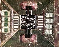
A project between Newcastle University and industry is aiming to spark a world electronics revolution by producing faster, cheaper and more reliable microchips. The University of Newcastle upon Tyne has joined forces with Atmel, based on North Tyneside in the North East of England, to create 'strained silicon' microchips, which involves adding a material called germanium to the traditional silicon used in semiconductor manufacturing. Atmel, whose silicon chips find applications in such diverse products as smart cards and game consoles like XBOX, is playing host to a team of five Newcastle University researchers led by top microelectronics professor Anthony O'Neill. "With this process we can create strained silicon microchips, which will be much faster or use less battery power than conventional microchips," explained Professor Anthony O'Neill, who leads a team of 5 researchers. The team, hosted by Atmel, aim to produce the world's first strained silicon technology, ahead of the competition. "Microchips have doubled in performance every 18 months for the last 30 years, but the end of the road is now in sight, which means new innovations like strained silicon are needed at the leading edge of microelectronics," added Professor O'Neill, l who has been working with strained silicon processes for almost ten years. Atmel Managing Director Craig McInnes said: "This is great news for the North East because it brings real, commercial research and development to the region. This will help develop the knowledge-based economy which is vital for our future. "We have the potential here for developing a brand new process which will give us cheaper and faster chips. These will be the market leaders of tomorrow. Atmel and Newcastle University have joined forces to develop some of the world's fastest microchips." The research and development project is based at Atmel's North Tyneside semiconductor factory and involves joint working to unravel the complexities of working with a new material called strained silicon germanium. Strained silicon on silicon-germanium has been tipped as one of the key emergent technologies for the next generation of semiconductors. If the venture proves successful it will bring leading edge technology to the North East. The two sides have entered in to a joint collaborative agreement and will share the fruits of the development if it proves to be a world beater. Atmel will supply the manufacturing know-how to speed up the development. The joint venture marks a break-though in collaborative working between Newcastle University and industry. Prof O'Neill added: "This really is getting the research out of the lab into the commercial world. Working with Atmel will allow us to take the product from the drawing board to marketable reality a lot quicker than relying on the limited resources available to universities. "Getting products to market quickly is vital in the fast-moving world of semiconductor manufacturing and development. If we are successful we will have a world first made on Tyneside." Strained Si CMOS technology can improve current logic technology without the expense of costly re-tooling or improve bleeding edge technology beyond state-of-the-art. Potential applications include low power chips, analog and low noise RF components. It will compete on the boundaries of high performance but more costly technologies (GaAs), enabling for example all silicon mobile communications products. It is compatible with, and complementary to, other contemporary technology innovations, e.g. copper interconnect, low-k dielectrics, metal gates, SoI, etc. The strain increases electron mobility leading to higher current in transistors. It is achieved by aligning atoms in a silicon film of thickness 10-30 nm with an underlying thick layer of unstrained silicon germanium (SiGe) alloy. Tensile strain in the silicon layer is engineered by the germanium concentration, which increases the separation of atoms in the alloy. Strained Si technology, aimed at the large CMOS market, differs from existing SiGe technology (in production by Atmel and others) used to engineer energy band gaps and so increase the gain of heterojunction bipolar transistors. Particular challenges relate to the high temperatures used in CMOS processing and the limited thickness of strained silicon possible due to its strain energy. Related Links Newcastle University SpaceDaily Search SpaceDaily Subscribe To SpaceDaily Express  Moffett Field - Nov 26, 2002
NASA scientists have invented a breakthrough biological method to make ultra-small structures that may well be used to produce electronics 10 to 100 times smaller than today's components.
|
| ||||||||||
| The content herein, unless otherwise known to be public domain, are Copyright 1995-2016 - Space Media Network. All websites are published in Australia and are solely subject to Australian law and governed by Fair Use principals for news reporting and research purposes. AFP, UPI and IANS news wire stories are copyright Agence France-Presse, United Press International and Indo-Asia News Service. ESA news reports are copyright European Space Agency. All NASA sourced material is public domain. Additional copyrights may apply in whole or part to other bona fide parties. Advertising does not imply endorsement, agreement or approval of any opinions, statements or information provided by Space Media Network on any Web page published or hosted by Space Media Network. Privacy Statement All images and articles appearing on Space Media Network have been edited or digitally altered in some way. Any requests to remove copyright material will be acted upon in a timely and appropriate manner. Any attempt to extort money from Space Media Network will be ignored and reported to Australian Law Enforcement Agencies as a potential case of financial fraud involving the use of a telephonic carriage device or postal service. |