|
|
| . |  |
. |
|
|
by Staff Writers Providence RI (SPX) Mar 07, 2013
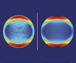
A multi-university research team has used a new spectroscopic method to gain a key insight into how light is emitted from layered nanomaterials and other thin films. The technique, called energy-momentum spectroscopy, enables researchers to look at the light emerging from a thin film and determine whether it is coming from emitters oriented along the plane of the film or from emitters oriented perpendicular to the film. Knowing the orientations of emitters could help engineers make better use of thin-film materials in optical devices like LEDs or solar cells. The research, published online on March 3 in Nature Nanotechnology, was a collaborative effort of Brown University, Case Western Reserve University, Columbia University, and the University of California-Santa Barbara. The new technique takes advantage of a fundamental property of thin films: interference. Interference effects can be seen in the rainbow colors visible on the surface of soap bubbles or oil slicks. Scientists can analyze how light constructively and destructively interferes at different angles to draw conclusions about the film itself - how thick it is, for example. This new technique takes that kind of analysis one step further for light-emitting thin films. "The key difference in our technique is we're looking at the energy as well as the angle and polarization at which light is emitted," said Rashid Zia, assistant professor of engineering at Brown University and one of the study's lead authors. "We can relate these different angles to distinct orientations of emitters in the film. At some angles and polarizations, we see only the light emission from in-plane emitters, while at other angles and polarizations we see only light originating from out-of-plane emitters." The researchers demonstrated their technique on two important thin-film materials, molybdenum disulfide (MoS2) and PTCDA. Each represents a class of materials that shows promise for optical applications. MoS2 is a two-dimensional material similar to graphene, and PTCDA is an organic semiconductor. The research showed that light emission from MoS2 occurs only from in-plane emitters. In PTCDA, light comes from two distinct species of emitters, one in-plane and one out-of-plane. Once the orientation of the emitters is known, Zia says, it may be possible to design structured devices that maximize those directional properties. In most applications, thin-film materials are layered on top of each other. The orientations of emitters in each layer indicate whether electronic excitations are happening within each layer or across layers, and that has implications for how such a device should be configured. "If you were making an LED using these layered materials and you knew that the electronic excitations were happening across an interface," Zia said, "then there's a specific way you want to design the structure to get all of that light out and increase its overall efficiency." The same concept could apply to light-absorbing devices like solar cells. By understanding how the electronic excitations happen in the material, it could be possible to structure it in a way that coverts more incoming light to electricity. "One of the exciting things about this research is how it brought together people with different expertise," Zia said. "Our group's expertise at Brown is in developing new forms of spectroscopy and studying the electronic origin of light emission. "The Kymissis group at Columbia has a great deal of expertise in organic semiconductors, and the Shan group at Case Western has a great deal of expertise in layered nanomaterials. "Jon Schuller, the study's first author, did a great job in bringing all this expertise together. Jon was a visiting scientist here at Brown, a postdoctoral fellow in the Energy Frontier Research Center at Columbia, and is now a professor at UCSB." Other authors on the paper were Sinan Karaveli (Brown), Theanne Schiros (Columbia), Keliang He (Case Western), Shyuan Yang (Columbia), Ioannis Kymissis (Columbia) and Jie Shan (Case Western). Funding for the work was provided by the Air Force Office of Scientific Research, the Department of Energy, the National Science Foundation, and the Nanoelectronic Research Initiative of the Semiconductor Research Corporation.
Related Links Brown University Nano Technology News From SpaceMart.com Computer Chip Architecture, Technology and Manufacture
|
|
| The content herein, unless otherwise known to be public domain, are Copyright 1995-2014 - Space Media Network. AFP, UPI and IANS news wire stories are copyright Agence France-Presse, United Press International and Indo-Asia News Service. ESA Portal Reports are copyright European Space Agency. All NASA sourced material is public domain. Additional copyrights may apply in whole or part to other bona fide parties. Advertising does not imply endorsement,agreement or approval of any opinions, statements or information provided by Space Media Network on any Web page published or hosted by Space Media Network. Privacy Statement |
 del.icio.us
 Digg
Digg Reddit
 Google