| . |  |
. |
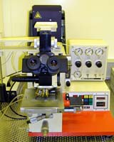
New York (UPI) Aug 30, 2005 Fountain pens that write on the nanometer scale could help create advanced microchips or medical and genetic devices, experts told UPI's Nano World. "We believe the technology will likely lead to many high-impact applications in the field of nanosensors, biotechnology and pharmaceuticals," said researcher Horacio Espinosa, an engineer at Northwestern University in Evanston, Ill. Nanotechnologists worldwide are experimenting with a method called dip-pen lithography, which can inscribe surfaces with nanometer precision. The technology could produce microchips with more circuits than before and thus more computing power or print biomolecules in arrays that could help sequence genes more rapidly or scan blood for diseases. Dip-pen lithography employs atomic-force microscopes, which run extraordinarily sharp probes across surfaces to scan them with three-dimensional molecular detail, much as a blind person uses his or her fingers to read bumps on a page of Braille. Dip-pen lithography coats these probes with any kind of ink scientists can devise -- for instance, semiconductor fluids or DNA -- and then employs these probes as writing quills. There is one problem: Dip-pen lithography replenishes ink by removing the probes from their writing surfaces and dipping them into wells, a constant stream of interruptions that limits throughput. Researchers have attempted to overcome this challenge by using micro-eyedroppers as pens, but the hitch is the ink typically ends up pooling around the micro-eyedropper tips, leading to wider lines than desired. Espinosa and his team solved this problem via silicon nitride fountain pens. Picture two hollow cones nested one inside the other. If the outer cone's tip is cut off and ink is poured into the space between the cones, the ink will end up coating only the inner cone's tip. The researchers created fountain pens with tips 50 to 100 nanometers wide that can draw features as small as 40 nanometers across, roughly the size of the smallest viruses found in nature. These "nano-fountain probes" are microfabricated using conventional techniques, which is key "to provide scalability to massively parallel arrays of probes," Espinosa explained. "This work is an exciting milestone for the field of probe-based lithography," said Craig Prater, director of technology development at atomic force microscope world leader Veeco Metrology in Santa Barbara, Calif. "Professor Espinosa's group has solved a major limitation with existing dip pen nanolithography." Espinosa and colleagues published their research in the scientific journal Small. The microfabrication techniques behind the nano-fountain probes are patented, and Northwestern currently is seeking to license the technology. Charles Choi covers research and technology for UPI. All rights reserved. � 2005 United Press International. Sections of the information displayed on this page (dispatches, photographs, logos) are protected by intellectual property rights owned by United Press International.. As a consequence, you may not copy, reproduce, modify, transmit, publish, display or in any way commercially exploit any of the content of this section without the prior written consent of United Press International. Related Links SpaceDaily Search SpaceDaily Subscribe To SpaceDaily Express  Stanford CA (SPX) Aug 31, 2005
One of the great challenges in the field of nanotechnology is optical imaging--specifically, how to design a microscope that produces high-resolution images of the nano-sized objects that researchers are trying to study.
|
| ||||||||||
| The content herein, unless otherwise known to be public domain, are Copyright 1995-2016 - Space Media Network. All websites are published in Australia and are solely subject to Australian law and governed by Fair Use principals for news reporting and research purposes. AFP, UPI and IANS news wire stories are copyright Agence France-Presse, United Press International and Indo-Asia News Service. ESA news reports are copyright European Space Agency. All NASA sourced material is public domain. Additional copyrights may apply in whole or part to other bona fide parties. Advertising does not imply endorsement, agreement or approval of any opinions, statements or information provided by Space Media Network on any Web page published or hosted by Space Media Network. Privacy Statement All images and articles appearing on Space Media Network have been edited or digitally altered in some way. Any requests to remove copyright material will be acted upon in a timely and appropriate manner. Any attempt to extort money from Space Media Network will be ignored and reported to Australian Law Enforcement Agencies as a potential case of financial fraud involving the use of a telephonic carriage device or postal service. |