| . |  |
. |
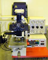
New approaches to building microchips are needed to keep computer power steadily advancing as it has for the past 30 years, and that means chip features must shrink to the order of nanometers -- or billionths of a meter. There are 10 methods competing for market share in this multibillion-dollar industry sector. Scientists have used every trick in the book to wring every last bit of performance out of processors used today, but it really does appear as if a new platform is needed, Matthew Nordan, vice president of research at nanotechnology analyst firm Lux Research in New York, told United Press International. The most critical step in chip building is the process of lithography, which lays down the pattern of desired chips on a silicon wafer. Lithography is the single most expensive part of the semiconductor manufacturing process, accounting for one-third of the cost of each chip today, Nordan said. It's also the bottleneck that stands to limit the power of microprocessors and the capacity of memory chips. With $3.9 billion in lithography tools sold last year, it's no surprise that 10 different platforms are now competing to take over when today's process runs out of steam. Today's standard method of patterning high-performance chips projects a column of light through lenses and a mask, which has the transistor features drawn on it, to a light-sensitive photoresist layer atop a silicon wafer. Dubbed optical projection lithography, this technique employs 193-nanometer wavelength lasers. Lux Research senior associate Will Arora said the 193-nanometer OPL is on its last stand. The practical limit for semiconductor feature size, due to physical constraints such as the angle of the optics, is about one-third of the wavelength used to pattern the chips, or about 65 nanometers for 193-nanometer OPL. Intel already began shipping Pentium 4 chips with 90-nanometer-wide transistors in February, and by 2007, 193-nanometer OPL will fail to keep up with Moore's Law -- the chip industry's ability to double transistor density every 18 months -- true since 1975. The buildup of heat in electronics makes raising the operating rate of chips impractical, with Intel in October canceling plans to increase the clock speed of its Pentium processors beyond 3.8 gigahertz. This means the only way chipmakers can sustain Moore's law is to put more circuits in less space, Nordan said. Lux researchers looked at 10 next-generation nanolithography platforms, all of which focus on patterning circuits smaller than 100 nanometers. Seven are optically based, much like 193-nanometer OPL, save they often use smaller wavelength light for proportionately tinier features. Two replace light with electrons, since electrons have wavelengths of less than a single nanometer. The final actually physically stamps features onto chips. The method industry will adopt en masse in 2008 as a stopgap solution until 2011 will be 193-nanometer liquid immersion lithography, the Lux team found. The reason for its popularity is that it is much like 193-nanometer OPL, but with a layer of water between the last lens and the wafer. The water bends the light at a sharper angle, allowing for finer features, Arora told UPI. Lux researchers said it should prove the least disruptive of the 10 contenders. In August, trade association Sematech threw its weight behind 193-nanometer liquid immersion lithography and Intel, IBM and Texas Instruments will all conduct trials this year. Lithography market leaders ASML, Canon and Nikon will begin plans to ship commercial immersion lithography tools by 2006. The problem is this immersion lithography tool will only hold out down to 45 nanometers at 2010, or 40 nanometers at 2011 at the latest if researchers come up with a liquid better than water for use in the system. Semiconductor industry players will need to prepare for a radically new platform, Arora said. Three contenders are neck and neck for the industry once immersion lithography runs out of steam. Lux researchers said at the moment, they believe nanoimprint lithography is in the lead. The technique presses a hard mask into a photoresist to stamp the pattern physically. It does not use expensive and cumbersome optics or lasers, making it simple and cheap, and it creates perfect patterns down to 10 nanometer lines. In 2002 Motorola became the first large semiconductor manufacturer to test a nanoimprint tool, and key infrastructure companies like KLA Tencor and LAM Research, vital to supporting any new lithography technique, have begun signing partnerships with nanoimprint vendors. The problem is that shifting from familiar optical methods to a non-optical one is a huge change from what's used today. Nanoimprint is a disruptive technology. It has a much higher burden of proof. For instance, defect rates from nanoimprint are unknown. There are five companies racing to commercialize nanoimprint -- EVG, Molecular Imprints, Nanonex, Obducat, and SUSS MicroTec. Arora said for nanoimprint to succeed, they need to form a consortium to advance their common interests and battle skepticism from major chipmakers. Two rivals for nanoimprint are extreme ultraviolet and X-ray projection. Extreme ultraviolet has long remained the leader, but over the past year industry support has declined due to technical obstacles with it that researchers at IBM, Sandia, Nikon, Intel, Canon and others have struggled with for two decades. People have repeatedly said that it would be ready in as little as four years for the last decade, Arora said. The wildcard is Adelphi Technology in Palo Alto, Calif., a little company at the early stages of developing X-ray projection, which is much like OPL, save it uses 1 nanometer X-rays instead of laser light. Their impact could be massive. But they have no presence. The giants like Intel should be returning their calls, Arora said. They are an extremely high-risk, high-reward option. Lux researchers predicted half the remaining six contenders -- electron projection, X-ray proximity and maskless optical -- likely will only be used for small-volume production, with their low costs off-setting their weaknesses in resolution or throughput. They believe the other three candidates -- 157 nanometer OPL, 157 nanometer liquid immersion, and parallel electron beam direct write -- are dead ends that will not be further developed due to lack of major industry support or low throughput. In any case, none of the contenders for long-term success in lithography use conventional optics. Companies making the optics currently used should identify new ways to remain relevant, Arora said. Optics company Carl Zeiss has recognized this potential shift, and has taken an equity stake in Molecular Imprints, one of the five companies in nanoimprint. It's a fairly cheap mechanism to make the shift, Nordan said. All rights reserved. Copyright 2004 by United Press International. Sections of the information displayed on this page (dispatches, photographs, logos) are protected by intellectual property rights owned by United Press International. As a consequence, you may not copy, reproduce, modify, transmit, publish, display or in any way commercially exploit any of the content of this section without the prior written consent of by United Press International. Related LinksSpaceDaily Search SpaceDaily Subscribe To SpaceDaily Express 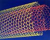 Canberra, Australia (SPX) Nov 19, 2004
In a collaborative effort, scientists at CSIRO Textile and Fibre Technology (CTFT) have achieved a major technological breakthrough that should soon lead to the production of futuristic strong, light and flexible 'smart' clothing materials.
|
| ||||||||||
| The content herein, unless otherwise known to be public domain, are Copyright 1995-2016 - Space Media Network. All websites are published in Australia and are solely subject to Australian law and governed by Fair Use principals for news reporting and research purposes. AFP, UPI and IANS news wire stories are copyright Agence France-Presse, United Press International and Indo-Asia News Service. ESA news reports are copyright European Space Agency. All NASA sourced material is public domain. Additional copyrights may apply in whole or part to other bona fide parties. Advertising does not imply endorsement, agreement or approval of any opinions, statements or information provided by Space Media Network on any Web page published or hosted by Space Media Network. Privacy Statement All images and articles appearing on Space Media Network have been edited or digitally altered in some way. Any requests to remove copyright material will be acted upon in a timely and appropriate manner. Any attempt to extort money from Space Media Network will be ignored and reported to Australian Law Enforcement Agencies as a potential case of financial fraud involving the use of a telephonic carriage device or postal service. |