| . |  |
. |
Tegal Corporation Thursday announced that it has been granted United States Patents, No. 6,689,220 and 6,756,318, which enable nano layer deposition (NLD) of conformal thin films for barrier, copper seed and high-K dielectric applications in advanced microprocessor and memory device production. The systems and methods described in the '220 and the '318 enable nano layer deposition with ultra-conformality comparable to that of atomic layer deposition (ALD) and the manufacturing throughput of more conventional chemical vapor deposition (CVD) systems. NLD allows semiconductor manufacturers to choose from a wide field of deposition precursors (a key limitation of ALD) for the application of any thin film in use today on the surface of a wafer with atomic layer precision. NLD technology can also be used to construct complex, compound film structures with a level of control and conformality that was previously unavailable or impractical. The '220 patent covers a system and process incorporating a pulsed plasma and deposition technique applicable to a variety of films such as Titanium Nitride, Copper and several low-K (dielectric constant) insulating films. The pulsing technique can also be used to deposit a low-K material and to "seal" it in-situ in order to preserve the film's low-K properties. This has been a major limitation to the successful implementation of low-K dielectric materials into current generations of semiconductors. The '318 patent combines system design, source design and NLD technology to enable a manufacturing solution for next generation semiconductor devices. The '318 discloses a new helical ribbon electrode as a plasma source for use in an NLD system. The '318 patent builds on the technology disclosed in the '220 patent and provides a multi-chamber platform for performing a wide variety of processing steps such as pre-clean, etch, NLD, densification, etc. As a result, complex films can be deposited with complete conformality and layer thicknesses can be controlled to one monolayer or to several hundred of Angstroms. The market for highly conformal deposition tools, such as ALD and NLD, is one of the fastest-growing segments of the semiconductor device manufacturing space. According to VLSI Research Inc., the current market for highly conformal deposition tools is over US$100 million and will grow at an annual rate of over 66% to reach US$1.35 billion in 2008. "We are pleased to add these two key patents to Tegal's extensive base of intellectual property and know-how," said Michael Parodi, Tegal chairman, president & CEO. "This is one of the most exciting areas that Tegal has ever participated in, and we look forward to demonstrating the superiority of our NLD systems in the market." Related Links Tegal SpaceDaily Search SpaceDaily Subscribe To SpaceDaily Express  Ann Arbor MI (SPX) Jul 22, 2004
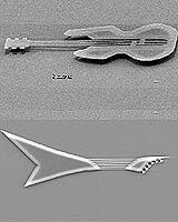
James Bond-style technologies such as cell phones the size of earpieces and invisible sensors sprinkled about to detect toxins are closer to reality. University of Michigan researchers have figured out how to build wireless systems even smaller while still retaining range and power efficiency.
|
| ||||||||||
| The content herein, unless otherwise known to be public domain, are Copyright 1995-2016 - Space Media Network. All websites are published in Australia and are solely subject to Australian law and governed by Fair Use principals for news reporting and research purposes. AFP, UPI and IANS news wire stories are copyright Agence France-Presse, United Press International and Indo-Asia News Service. ESA news reports are copyright European Space Agency. All NASA sourced material is public domain. Additional copyrights may apply in whole or part to other bona fide parties. Advertising does not imply endorsement, agreement or approval of any opinions, statements or information provided by Space Media Network on any Web page published or hosted by Space Media Network. Privacy Statement All images and articles appearing on Space Media Network have been edited or digitally altered in some way. Any requests to remove copyright material will be acted upon in a timely and appropriate manner. Any attempt to extort money from Space Media Network will be ignored and reported to Australian Law Enforcement Agencies as a potential case of financial fraud involving the use of a telephonic carriage device or postal service. |