| . |  |
. |
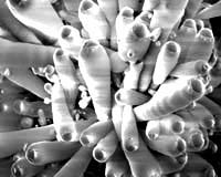
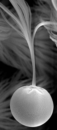
Using molten gallium as a catalyst, researchers at the Georgia Institute of Technology have simultaneously grown hundreds of thousands of silica nanowires from each micron-scale catalyst droplet. Bundles of the highly aligned and closely packed nanowires form unusual structures resembling cones, cherries, carrots and comets. Use of gallium catalysts could facilitate high-volume production of silica (SiO2) nanowires, improving the vapor-liquid-solid (VLS) process now used to make the structures. The gallium catalysts also produce nanowires that spontaneously divide into branching structures that could have potential applications as optical splitters in nanometer-scale photonic systems. The National Science Foundation-sponsored work was reported in the February 2002 issue of the Journal of the American Chemical Society. "These nanowires demonstrate many amazing growth phenomena unlike any previously observed through a conventional VLS growth process," explained Zhong Lin Wang, director of the Georgia Tech Center for Nanoscience and Nanotechnology, and a professor of materials science and engineering. "These silica nanowires could have applications ranging from optics to surface coatings. It's my hope that they can be useful as small-scale optical fibers useful for splitting a signal." The ability to grow large bundles of aligned nanowires from a single catalyst could help lower production costs, potentially opening up new applications for the structures. In standard VLS synthesis techniques used for producing silica nanowires, each wire grows from a single particle of gold, cobalt, nickel or other high melting point metal. Vapor-phase silicon evaporated from a wafer inside a high-temperature furnace condenses on the surface of the molten catalyst, where it combines with oxygen and crystallizes to form silica nanowires. In the standard process, the size of the catalytic particle controls the diameter of the nanowire grown from it. Because the wires grow individually from the catalyst particles, they produce tangled masses of varying lengths. But by using droplets of gallium 5 to 50 microns in diameter -- thousands of times larger than standard catalytic particles -- Wang and collaborators Zheng Wei Pan, Zu Rong Dai and Chris Ma grow hundreds of thousands of nanowires from a single catalyst. The nanowires attached to each droplet grow to approximately the same length, and remain well ordered, aligned to form hollow macro-scale structures that resemble snowy-white cones, carrots, cherries or comets. "The importance of this process is that it will allow us to grow many aligned wires rather than tangles of wires," said Wang. "The uniformity of the wires produced in this way could be very useful." Some of the nanowires spontaneously split into branches, often more than once, with the diameters of the branches equal. "This is very different from any existing types of nanowires," said Wang. "This branching ability makes it possible to produce junctions that may have applications to light propagation."
Formation of the nanowires takes place in a high-temperature tube furnace. Gallium nitride powder is placed in a crucible located in the center of an alumina tube with a long silicon wafer stripe nearby atop an alumina plate. As argon gas is flowed through the furnace, the gallium nitride is heated to approximately 1,150 Celsius, which causes the powder to decompose into molten clusters of metal and nitrogen gas. The liquid gallium clusters agglomerate, forming droplets large enough to be visible inside the furnace. Carried by the argon flowing through the furnace, the droplets condense on the silicon wafer. The hot gallium stimulates the vaporization of silicon from the wafer, then serves as a catalyst for a reaction between the silicon vapor and oxygen to form silica. Over a period of five hours, bundles of silica nanowires form between the gallium droplets and the surface of the wafer, pushing the gallium upward. Silica nanowires with somewhat different properties also form between gallium droplets and alumina surfaces inside the furnace. On the silicon substrate, the wires have diameters of 15-30 nanometers and lengths of 10-40 microns. On the alumina substrate, the silica nanowires are larger, with diameters of 50-100 nanometers and lengths of 10-50 microns. Silica nanowires produced by the standard VLS process are composed of a single crystal. Nanowires produced by the gallium catalyst are composed of amorphous silica. Beyond investigating the optical properties of the silica nanowires, Wang hopes next to investigate whether the gallium catalyst system can be used to produce other nanostructures. Related Links School of Materials Science & Engineering at Georgia Institute SpaceDaily Search SpaceDaily Subscribe To SpaceDaily Express  Boston - Feb 14, 2002
A future filled with tiny, molecule-sized computers-fast and powerful enough to do things like translate conversations on the fly or calculate complex climate models-may be closer than people think, top nanotechnology researchers said at the American Association for the Advancement of Science (AAAS) Annual Meeting in Boston today.
|
| |||||||||||
| The content herein, unless otherwise known to be public domain, are Copyright 1995-2016 - Space Media Network. All websites are published in Australia and are solely subject to Australian law and governed by Fair Use principals for news reporting and research purposes. AFP, UPI and IANS news wire stories are copyright Agence France-Presse, United Press International and Indo-Asia News Service. ESA news reports are copyright European Space Agency. All NASA sourced material is public domain. Additional copyrights may apply in whole or part to other bona fide parties. Advertising does not imply endorsement, agreement or approval of any opinions, statements or information provided by Space Media Network on any Web page published or hosted by Space Media Network. Privacy Statement All images and articles appearing on Space Media Network have been edited or digitally altered in some way. Any requests to remove copyright material will be acted upon in a timely and appropriate manner. Any attempt to extort money from Space Media Network will be ignored and reported to Australian Law Enforcement Agencies as a potential case of financial fraud involving the use of a telephonic carriage device or postal service. |