| . |  |
. |
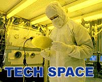
A decades-old, X-ray-based method for studying the atomic structure of materials may be the answer to a looming semiconductor industry need--a rugged, high-throughput technology for measuring dimensions of chip circuitry packed with devices approaching molecular proportions. A team led by National Institute of Standards and Technology (NIST) scientists recently reported* their initial success in adapting small- angle X-ray scattering (SAXS) to rapidly characterize the size and shape of grid-like patterns with nanometer-scale linewidths. With better than one nanometer (billionth of a meter) precision, the team determined the average size of periodically repeating features arrayed on three chemically different samples much like the intricately patterned polymer masks used to print integrated-circuit designs. With the size of on-chip devices soon to shrink to below 100 nanometers, current dimensional measurement tools are approaching their limits. The versatile SAXS method, the team suggests, could be an able substitute. It can be used on a wide range of materials to evaluate the quality of surface and subsurface patterns consisting of features considerably smaller than 100 nanometers. In proof-of-concept experiments supported by the Defense Advanced Research Projects Agency, NIST, and the U.S. Department of Energy, essential data were gathered, within a second, over an area about 40 micrometers on a side--a large swath, nanotechnologically speaking. Images assembled from X-rays deflected by electrons in the samples yielded high-precision measurements of linewidths, spaces, line-edge roughness, and feature geometry. Implementing the SAXS method actually should become easier as feature sizes decrease and near molecular dimensions, explains NIST's Ronald Jones. Related Links National Institute of Standards and Technology SpaceDaily Search SpaceDaily Subscribe To SpaceDaily Express When amazing new computers and other electronic devices emerge, they will have been conceived and incubated in university laboratories like that of Dr. Chris Gorman, professor of chemistry at North Carolina State University. There, the scientist and his multidisciplinary team are working to build, molecule by molecule, a nanoscale transistor.
|
| ||||||||||
| The content herein, unless otherwise known to be public domain, are Copyright 1995-2016 - Space Media Network. All websites are published in Australia and are solely subject to Australian law and governed by Fair Use principals for news reporting and research purposes. AFP, UPI and IANS news wire stories are copyright Agence France-Presse, United Press International and Indo-Asia News Service. ESA news reports are copyright European Space Agency. All NASA sourced material is public domain. Additional copyrights may apply in whole or part to other bona fide parties. Advertising does not imply endorsement, agreement or approval of any opinions, statements or information provided by Space Media Network on any Web page published or hosted by Space Media Network. Privacy Statement All images and articles appearing on Space Media Network have been edited or digitally altered in some way. Any requests to remove copyright material will be acted upon in a timely and appropriate manner. Any attempt to extort money from Space Media Network will be ignored and reported to Australian Law Enforcement Agencies as a potential case of financial fraud involving the use of a telephonic carriage device or postal service. |