| . |  |
. |
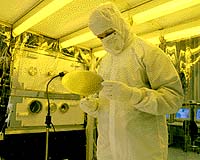
New methods reported recently by researchers from the Commerce Department's National Institute of Standards and Technology (NIST), the IBM T.J. Watson Research Center and the University of Texas at Austin will aid the semiconductor industry's urgent search for new photosensitive materials needed to print integrated-circuit patterns with features smaller than a hundred nanometers. Using X-ray and neutron probes, the team directly measured the spatial location of the complex chemical processes used to sculpt the transistors, lines, trenches and other minuscule components of the silicon-chip landscape. The almost-molecular level view of a model system afforded by their methods enabled the researchers to directly link the reaction front along chemically amplified photoresists to the profile and composition of the final developed, or "printed," structure. Writing in the July 19, 2002, issue of Science, the researchers point out that, in 2003, the semiconductor industry aims to produce chips with feature sizes, or "critical dimensions," that are smaller than 100 nanometers (billionths of a meter), as compared with 130 nanometers today. Reaching that target -- and continuing the industry's decades-long run of doubling the number of devices on a chip about every 18 months (known as "Moore's Law") -- leaves almost no room for error. "The critical dimensions must be controlled," the team notes in the paper, "to within 2 to 5 nanometers which is comparable to the characteristic size of the (individual) polymeric molecules in the photoresists used to pattern the features." Chemically amplified photoresists, in fact, were a key innovation in a string of photolithography advances over the years. These innovations have perpetuated the industry's use of light and stencil-like masks to print chip patterns, even as feature sizes have shrunk to less than the shortest wavelength of visible light. Photoresists are light-sensitive polymer films that coat the silicon wafers used to make chips. Parts of the film exposed to light beamed through the patterned mask become soluble and can be washed away. During further processing, exposed areas are adorned with the tiny interconnected components that make up the chip circuitry. Chemical amplification is akin to a light-triggered etching process. Light releases acid molecules that, during heating, spread across the exposed areas of the photoresist. As it diffuses, the acid catalyzes a reaction, removing protectant groups from the photoresist in a "deprotection front" that alters the solubility in a developer solution of parts of the photoresist bordering the front. The complex process has yielded sufficiently well-defined patterns for chipmaking up until now. "Current understanding of the process," says NIST polymer scientist Eric K. Lin, who led the research effort, "is not sufficiently detailed to ensure that it can be used to reliably achieve the resolution necessary to make semiconductors with sub-100-nanometer feature sizes." If, for example, the acid molecules diffuse too far, then the reaction front will be poorly defined, the resultant pattern will be blurred, and, ultimately, on-chip devices will not meet nanometer-level tolerances. In addition, the researchers write, next-generation semiconductors will be made with thinner photoresist films. This adjustment could affect photoresist properties and influence the formation and movement of the pattern-forming deprotection front, they say. With the methods developed by Lin and his colleagues, the semiconductor industry has a direct means to resolve these and other important unknowns, moving them out of the realm of trial-and-error experimentation. Measurements of beams of X-rays and beams of neutrons reflected off model photoresist layers before, during and after the deprotection reaction captured key details on the structure of the interface between the two layers, the profile and advance of the reaction front, local changes in chemical composition, and other important aspects of the process. The researchers found, for example, that the ultimate position of a feature on the pattern printed on a photoresist was offset from a predicted location of the reaction front. Although the difference of three nanometers did not exceed the estimated tolerance for next-generation chips, other sources of error might combine with the offset to exceed the limit. Challenges also may arise when the reaction front spans the entire perimeter of a pattern structure in the making. "Actual fabrication of sub-100 nanometer lines would involve two opposing reaction fronts that may interact and affect the dimensions of the patterned structure," the article says. Measurement methods developed by the NIST-led team "fill a significant gap in the study, design and simulation of photoresist materials," Lin says. "Fundamental mechanisms can be investigated and computer simulation software can be directly tested with high-resolution data. This, we hope, will lead to materials that are optimized for what must be an extremely precise manufacturing process." A non-regulatory agency of the U.S. Department of Commerce's Technology Administration, NIST develops and promotes measurement, standards and technology to enhance productivity, facilitate trade and improve the quality of life. Related Links National Institute of Standards and Technology SpaceDaily Search SpaceDaily Subscribe To SpaceDaily Express  Madison - Jul 26, 2002
Material scientists at the University of Wisconsin at Madison have built a semiconductor based device that can trap individual electrons and line them up, an advance that could bring quantum computing out of the gee-whiz world of scientific novelty and into the practical realm.
|
| ||||||||||
| The content herein, unless otherwise known to be public domain, are Copyright 1995-2016 - Space Media Network. All websites are published in Australia and are solely subject to Australian law and governed by Fair Use principals for news reporting and research purposes. AFP, UPI and IANS news wire stories are copyright Agence France-Presse, United Press International and Indo-Asia News Service. ESA news reports are copyright European Space Agency. All NASA sourced material is public domain. Additional copyrights may apply in whole or part to other bona fide parties. Advertising does not imply endorsement, agreement or approval of any opinions, statements or information provided by Space Media Network on any Web page published or hosted by Space Media Network. Privacy Statement All images and articles appearing on Space Media Network have been edited or digitally altered in some way. Any requests to remove copyright material will be acted upon in a timely and appropriate manner. Any attempt to extort money from Space Media Network will be ignored and reported to Australian Law Enforcement Agencies as a potential case of financial fraud involving the use of a telephonic carriage device or postal service. |