| . |  |
. |
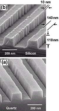
In a discovery that could greatly reduce the size and cost of computer chips, Princeton researchers have found a fast method for printing ultrasmall patterns in silicon wafers. The method, described in the June 20 issue of Nature, could allow electronics manufacturers to increase the density of transistors on silicon chips by 100-fold while dramatically streamlining the production process. Packing more transistors onto chips is the key to making more powerful computer processors and memory chips. Researchers in the lab of electrical engineer Stephen Chou used the new technique to make patterns with features measuring 10 nanometers -- 10 millionths of millimeter. The method involves pressing a mold against a piece of silicon and applying a laser pulse for just 20 billionths of a second. The surface of the silicon briefly melts and resolidifies around the mold. The method eliminates the costly and time-consuming step of etching, or photolithography, which had been the only way to make such small patterns in silicon. While the etching process takes 10 or 20 minutes to make a single chip, Chou's imprint method accomplishes it in a quarter of a millionth of a second. "Here you do not need to use all those steps," said Chou. "You just imprint the pattern directly into the silicon. You not only reduce the number of steps, you can do it in nanoseconds." Chou's co-authors on the paper are graduate students Chris Keimel and Jian Gu. In a commentary accompanying the research report in Nature, electrical engineer Fabian Pease of Stanford University wrote that the new method could allow electronics manufacturers to continue the rapid pace of miniaturization that has continued for three decades, but appeared to be running up against fundamental physical limits. Chou has made a career of breaking what had appeared to be physical limits of miniaturization. In 1996, he developed a method for imprinting nanometer-scale patterns into plastic polymers. That breakthrough greatly simplified the process of making molds, but costly etching was still required to transfer these patterns into silicon. Chou believed that imprinting would work directly in silicon and could be made to happen much faster. "People's intuition is that mechanical processes are very slow, so imprinting cannot be fast," said Chou. "But I knew there is no scientific proof of that. So how do you design an experiment to explore the speed limit of the imprint process?" The key turned out to be a tool called an excimer laser, which is commonly used in laser surgeries because it can heat just the thinnest surface layer of a material without causing damage underneath. Using conventional etching, Chou made a template of the pattern he wanted out of quartz, which is transparent to the laser beam, and pressed it against the silicon. A brief laser pulse melted the silicon surface around the mold. The silicon does not stick to the quartz. Revealed by electron microscopes, the patterns the researchers produced look like long, squared-off channels. Each ridge measures 140 nanometers across and is topped by a much smaller ridge just 10 nanometers wide. By comparison, a 10-nanometer ribbon next to a human hair would look like the lead of a mechanical pencil next to a train car. Chou dubbed the method Laser-Assisted Direct Imprint, or LADI. The University has begun the process of filing for a patent. Chou believes the LADI process will mesh well with another of his earlier breakthroughs, his creation in 1996 of the world's smallest transistor, which requires only a single electron of current. Making common use of such a small transistor has been inhibited by lack of a convenient manufacturing process, he said. Another benefit of LADI, said Chou, is that it eliminates the chemicals used in conventional lithography and is thus more environmentally friendly. In addition to its commercial applications, the discovery opens an interesting avenue of scientific research, said Chou. Understanding the physics behind melting and solidifying on such small scales will require input from many fields, including materials science, mechanics and microfluidics. "Scientifically, people are still trying to understand how it works, because it is amazing that it works at all," said Chou. Related Links Princeton SpaceDaily Search SpaceDaily Subscribe To SpaceDaily Express  Buffalo - May 20, 2002
A team of researchers led by University at Buffalo physicists reported today that they have created semiconducting materials that exhibit the key properties that are essential to the development of semiconductor spintronic devices.
|
| ||||||||||
| The content herein, unless otherwise known to be public domain, are Copyright 1995-2016 - Space Media Network. All websites are published in Australia and are solely subject to Australian law and governed by Fair Use principals for news reporting and research purposes. AFP, UPI and IANS news wire stories are copyright Agence France-Presse, United Press International and Indo-Asia News Service. ESA news reports are copyright European Space Agency. All NASA sourced material is public domain. Additional copyrights may apply in whole or part to other bona fide parties. Advertising does not imply endorsement, agreement or approval of any opinions, statements or information provided by Space Media Network on any Web page published or hosted by Space Media Network. Privacy Statement All images and articles appearing on Space Media Network have been edited or digitally altered in some way. Any requests to remove copyright material will be acted upon in a timely and appropriate manner. Any attempt to extort money from Space Media Network will be ignored and reported to Australian Law Enforcement Agencies as a potential case of financial fraud involving the use of a telephonic carriage device or postal service. |